M25PX64
64-Mbit, dual I/O, 4-Kbyte subsector erase,
serial flash memory with 75 MHz SPI bus interface
Features
SPI bus compatible serial interface
75 MHz (maximum) clock frequency
2.7 V to 3.6 V single supply voltage
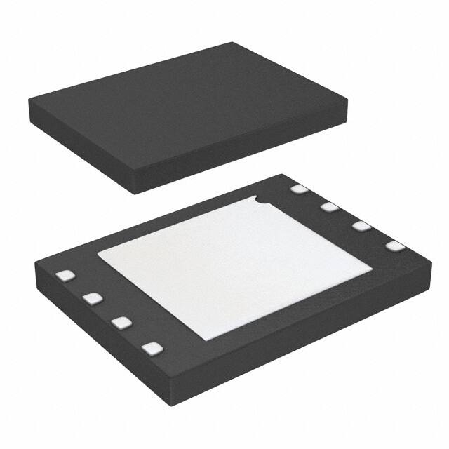
VDFPN8 (ME)
8 × 6 mm (MLP8)
Dual input/output instructions resulting in an
equivalent clock frequency of 150 MHz:
– Dual output fast read instruction
– Dual input fast program instruction
VDFPN8 (MD)
8 × 6 mm (MLP8)
(with reduced D2
dimension)
Whole memory continuously read by sending
once a fast read or a dual output fast read
instruction and an address
64 Mbit Flash memory
– Uniform 4-Kbyte subsectors
– Uniform 64-Kbyte sectors
SO16 (MF)
300 mils width
TBGA24 (ZM) 6x8 mm
Additional 64-byte user-lockable, one-time
programmable (OTP) area
Erase capability
– Subsector (4-Kbyte) granularity
– Sector (64-Kbyte) granularity
– Bulk erase (64 Mbits) in 68 s (typical)
Automotive Certified Parts Available
Write protections
– Software write protection applicable to
every 64-Kbyte sector (volatile lock bit)
– Hardware write protection: protected area
size defined by three non-volatile bits (BP0,
BP1 and BP2)
Deep power-down mode: 5 μA (typical)
Electronic signature
– JEDEC standard two-byte signature
(7117h)
– Unique ID code (UID) with 16 bytes readonly, available upon customer request
More than 100 000 write cycles per sector
More than 20 years data retention
Packages
– RoHS compliant
November 2009
Rev 10
1/70
www.numonyx.com
1
�Contents
M25PX64
Contents
1
Description . . . . . . . . . . . . . . . . . . . . . . . . . . . . . . . . . . . . . . . . . . . . . . . . . 6
2
Signal descriptions . . . . . . . . . . . . . . . . . . . . . . . . . . . . . . . . . . . . . . . . . . 9
2.1
Serial data output (DQ1) . . . . . . . . . . . . . . . . . . . . . . . . . . . . . . . . . . . . . . 9
2.2
Serial data input (DQ0) . . . . . . . . . . . . . . . . . . . . . . . . . . . . . . . . . . . . . . . . 9
2.3
Serial Clock (C) . . . . . . . . . . . . . . . . . . . . . . . . . . . . . . . . . . . . . . . . . . . . . 9
2.4
Chip Select (S) . . . . . . . . . . . . . . . . . . . . . . . . . . . . . . . . . . . . . . . . . . . . . . 9
2.5
Hold (HOLD) . . . . . . . . . . . . . . . . . . . . . . . . . . . . . . . . . . . . . . . . . . . . . . . . 9
2.6
Write protect/enhanced program supply voltage (W/VPP) . . . . . . . . . . . . 10
2.7
VCC supply voltage . . . . . . . . . . . . . . . . . . . . . . . . . . . . . . . . . . . . . . . . . . 10
2.8
VSS ground . . . . . . . . . . . . . . . . . . . . . . . . . . . . . . . . . . . . . . . . . . . . . . . . 10
3
SPI modes . . . . . . . . . . . . . . . . . . . . . . . . . . . . . . . . . . . . . . . . . . . . . . . . 11
4
Operating features . . . . . . . . . . . . . . . . . . . . . . . . . . . . . . . . . . . . . . . . . 13
4.1
Page programming . . . . . . . . . . . . . . . . . . . . . . . . . . . . . . . . . . . . . . . . . . 13
4.2
Dual input fast program . . . . . . . . . . . . . . . . . . . . . . . . . . . . . . . . . . . . . . 13
4.3
Subsector erase, sector erase and bulk erase . . . . . . . . . . . . . . . . . . . . . 13
4.4
Polling during a write, program or erase cycle . . . . . . . . . . . . . . . . . . . . . 13
4.5
Active power, standby power and deep power-down modes . . . . . . . . . . 13
4.6
Status register . . . . . . . . . . . . . . . . . . . . . . . . . . . . . . . . . . . . . . . . . . . . . 14
4.7
Protection modes . . . . . . . . . . . . . . . . . . . . . . . . . . . . . . . . . . . . . . . . . . . 15
4.8
4.7.1
Protocol-related protections . . . . . . . . . . . . . . . . . . . . . . . . . . . . . . . . . . 15
4.7.2
Specific hardware and software protection . . . . . . . . . . . . . . . . . . . . . . 16
Hold condition . . . . . . . . . . . . . . . . . . . . . . . . . . . . . . . . . . . . . . . . . . . . . . 18
5
Memory organization . . . . . . . . . . . . . . . . . . . . . . . . . . . . . . . . . . . . . . . 19
6
Instructions . . . . . . . . . . . . . . . . . . . . . . . . . . . . . . . . . . . . . . . . . . . . . . . 26
2/70
6.1
Write enable (WREN) . . . . . . . . . . . . . . . . . . . . . . . . . . . . . . . . . . . . . . . . 28
6.2
Write disable (WRDI) . . . . . . . . . . . . . . . . . . . . . . . . . . . . . . . . . . . . . . . . 29
6.3
Read identification (RDID) . . . . . . . . . . . . . . . . . . . . . . . . . . . . . . . . . . . . 30
�M25PX64
Contents
6.4
Read status register (RDSR) . . . . . . . . . . . . . . . . . . . . . . . . . . . . . . . . . . 32
6.4.1
WIP bit . . . . . . . . . . . . . . . . . . . . . . . . . . . . . . . . . . . . . . . . . . . . . . . . . . 32
6.4.2
WEL bit . . . . . . . . . . . . . . . . . . . . . . . . . . . . . . . . . . . . . . . . . . . . . . . . . 32
6.4.3
BP2, BP1, BP0 bits . . . . . . . . . . . . . . . . . . . . . . . . . . . . . . . . . . . . . . . . 32
6.4.4
Top/bottom bit . . . . . . . . . . . . . . . . . . . . . . . . . . . . . . . . . . . . . . . . . . . . 33
6.4.5
SRWD bit . . . . . . . . . . . . . . . . . . . . . . . . . . . . . . . . . . . . . . . . . . . . . . . . 33
6.5
Write status register (WRSR) . . . . . . . . . . . . . . . . . . . . . . . . . . . . . . . . . . 34
6.6
Read data bytes (READ) . . . . . . . . . . . . . . . . . . . . . . . . . . . . . . . . . . . . . 36
6.7
Read data bytes at higher speed (FAST_READ) . . . . . . . . . . . . . . . . . . . 37
6.8
Dual output fast read (DOFR) . . . . . . . . . . . . . . . . . . . . . . . . . . . . . . . . . 38
6.9
Read lock register (RDLR) . . . . . . . . . . . . . . . . . . . . . . . . . . . . . . . . . . . . 39
6.10
Read OTP (ROTP) . . . . . . . . . . . . . . . . . . . . . . . . . . . . . . . . . . . . . . . . . . 40
6.11
Page program (PP) . . . . . . . . . . . . . . . . . . . . . . . . . . . . . . . . . . . . . . . . . 41
6.12
Dual input fast program (DIFP) . . . . . . . . . . . . . . . . . . . . . . . . . . . . . . . . 43
6.13
Program OTP instruction (POTP) . . . . . . . . . . . . . . . . . . . . . . . . . . . . . . . 45
6.14
Write to lock register (WRLR) . . . . . . . . . . . . . . . . . . . . . . . . . . . . . . . . . . 47
6.15
Subsector erase (SSE) . . . . . . . . . . . . . . . . . . . . . . . . . . . . . . . . . . . . . . . 48
6.16
Sector erase (SE) . . . . . . . . . . . . . . . . . . . . . . . . . . . . . . . . . . . . . . . . . . . 49
6.17
Bulk erase (BE) . . . . . . . . . . . . . . . . . . . . . . . . . . . . . . . . . . . . . . . . . . . . 50
6.18
Deep power-down (DP) . . . . . . . . . . . . . . . . . . . . . . . . . . . . . . . . . . . . . . 51
6.19
Release from deep power-down (RDP) . . . . . . . . . . . . . . . . . . . . . . . . . . 52
7
Power-up and power-down . . . . . . . . . . . . . . . . . . . . . . . . . . . . . . . . . . 53
8
Initial delivery state . . . . . . . . . . . . . . . . . . . . . . . . . . . . . . . . . . . . . . . . . 54
9
Maximum ratings . . . . . . . . . . . . . . . . . . . . . . . . . . . . . . . . . . . . . . . . . . . 55
10
DC and AC parameters . . . . . . . . . . . . . . . . . . . . . . . . . . . . . . . . . . . . . . 56
11
Package mechanical . . . . . . . . . . . . . . . . . . . . . . . . . . . . . . . . . . . . . . . . 62
12
Ordering information . . . . . . . . . . . . . . . . . . . . . . . . . . . . . . . . . . . . . . . 67
13
Revision history . . . . . . . . . . . . . . . . . . . . . . . . . . . . . . . . . . . . . . . . . . . 69
3/70
�List of tables
M25PX64
List of tables
Table 1.
Table 2.
Table 3.
Table 4.
Table 5.
Table 6.
Table 7.
Table 8.
Table 9.
Table 10.
Table 11.
Table 12.
Table 13.
Table 14.
Table 15.
Table 16.
Table 17.
Table 18.
Table 19.
Table 20.
Table 21.
Table 22.
Table 23.
Table 24.
4/70
Signal names . . . . . . . . . . . . . . . . . . . . . . . . . . . . . . . . . . . . . . . . . . . . . . . . . . . . . . . . . . . . 7
Software protection truth table (sectors 0 to 127, 64-Kbyte granularity). . . . . . . . . . . . . . . 16
Protected area sizes . . . . . . . . . . . . . . . . . . . . . . . . . . . . . . . . . . . . . . . . . . . . . . . . . . . . . . 17
Memory organization . . . . . . . . . . . . . . . . . . . . . . . . . . . . . . . . . . . . . . . . . . . . . . . . . . . . . 20
Instruction set . . . . . . . . . . . . . . . . . . . . . . . . . . . . . . . . . . . . . . . . . . . . . . . . . . . . . . . . . . . 27
Read identification (RDID) data-out sequence . . . . . . . . . . . . . . . . . . . . . . . . . . . . . . . . . . 30
Status register format . . . . . . . . . . . . . . . . . . . . . . . . . . . . . . . . . . . . . . . . . . . . . . . . . . . . . 32
Protection modes . . . . . . . . . . . . . . . . . . . . . . . . . . . . . . . . . . . . . . . . . . . . . . . . . . . . . . . . 35
Lock register out . . . . . . . . . . . . . . . . . . . . . . . . . . . . . . . . . . . . . . . . . . . . . . . . . . . . . . . . . 39
Lock register in . . . . . . . . . . . . . . . . . . . . . . . . . . . . . . . . . . . . . . . . . . . . . . . . . . . . . . . . . . 47
Power-up timing and VWI threshold . . . . . . . . . . . . . . . . . . . . . . . . . . . . . . . . . . . . . . . . . . 54
Absolute maximum ratings . . . . . . . . . . . . . . . . . . . . . . . . . . . . . . . . . . . . . . . . . . . . . . . . . 55
Operating conditions. . . . . . . . . . . . . . . . . . . . . . . . . . . . . . . . . . . . . . . . . . . . . . . . . . . . . . 56
Data Retention and Endurance . . . . . . . . . . . . . . . . . . . . . . . . . . . . . . . . . . . . . . . . . . . . . 56
AC measurement conditions. . . . . . . . . . . . . . . . . . . . . . . . . . . . . . . . . . . . . . . . . . . . . . . . 56
Capacitance . . . . . . . . . . . . . . . . . . . . . . . . . . . . . . . . . . . . . . . . . . . . . . . . . . . . . . . . . . . . 57
DC characteristics. . . . . . . . . . . . . . . . . . . . . . . . . . . . . . . . . . . . . . . . . . . . . . . . . . . . . . . . 57
AC characteristics. . . . . . . . . . . . . . . . . . . . . . . . . . . . . . . . . . . . . . . . . . . . . . . . . . . . . . . . 58
VDFPN8 (MLP8, ME) 8-lead very thin dual flat package no lead,
8 × 6 mm, package mechanical data . . . . . . . . . . . . . . . . . . . . . . . . . . . . . . . . . . . . . . . . . 62
VDFPN8 (MLP8, MD) 8-lead very thin dual flat package no lead,
8 × 6 mm, package mechanical data . . . . . . . . . . . . . . . . . . . . . . . . . . . . . . . . . . . . . . . . . 63
SO16 wide - 16-lead plastic small outline, 300 mils body width, mechanical data . . . . . . . 64
TBGA 6x8 mm 24-ball package dimensions. . . . . . . . . . . . . . . . . . . . . . . . . . . . . . . . . . . . 66
Ordering information scheme . . . . . . . . . . . . . . . . . . . . . . . . . . . . . . . . . . . . . . . . . . . . . . . 67
Document revision history . . . . . . . . . . . . . . . . . . . . . . . . . . . . . . . . . . . . . . . . . . . . . . . . . 69
�M25PX64
List of figures
List of figures
Figure 1.
Figure 2.
Figure 3.
Figure 4.
Figure 5.
Figure 6.
Figure 7.
Figure 8.
Figure 9.
Figure 10.
Figure 11.
Figure 12.
Figure 13.
Figure 14.
Figure 15.
Figure 16.
Figure 17.
Figure 18.
Figure 19.
Figure 20.
Figure 21.
Figure 22.
Figure 23.
Figure 24.
Figure 25.
Figure 26.
Figure 27.
Figure 28.
Figure 29.
Figure 30.
Figure 31.
Figure 32.
Figure 33.
Figure 34.
Figure 35.
Figure 36.
Figure 37.
Figure 38.
Figure 39.
Logic diagram . . . . . . . . . . . . . . . . . . . . . . . . . . . . . . . . . . . . . . . . . . . . . . . . . . . . . . . . . . . . 7
VDFPN8 connections . . . . . . . . . . . . . . . . . . . . . . . . . . . . . . . . . . . . . . . . . . . . . . . . . . . . . . 7
SO16 connections . . . . . . . . . . . . . . . . . . . . . . . . . . . . . . . . . . . . . . . . . . . . . . . . . . . . . . . . 8
BGA 6x8 24 ball ballout . . . . . . . . . . . . . . . . . . . . . . . . . . . . . . . . . . . . . . . . . . . . . . . . . . . . 8
Bus master and memory devices on the SPI bus . . . . . . . . . . . . . . . . . . . . . . . . . . . . . . . . 11
SPI modes supported . . . . . . . . . . . . . . . . . . . . . . . . . . . . . . . . . . . . . . . . . . . . . . . . . . . . . 12
Hold condition activation. . . . . . . . . . . . . . . . . . . . . . . . . . . . . . . . . . . . . . . . . . . . . . . . . . . 18
Block diagram . . . . . . . . . . . . . . . . . . . . . . . . . . . . . . . . . . . . . . . . . . . . . . . . . . . . . . . . . . . 19
Write enable (WREN) instruction sequence . . . . . . . . . . . . . . . . . . . . . . . . . . . . . . . . . . . . 28
Write disable (WRDI) instruction sequence . . . . . . . . . . . . . . . . . . . . . . . . . . . . . . . . . . . . 29
Read identification (RDID) instruction sequence and data-out sequence . . . . . . . . . . . . . 31
Read status register (RDSR) instruction sequence and data-out sequence . . . . . . . . . . . 33
Write status register (WRSR) instruction sequence . . . . . . . . . . . . . . . . . . . . . . . . . . . . . . 34
Read data bytes (READ) instruction sequence and data-out sequence . . . . . . . . . . . . . . 36
Read data bytes at higher speed (FAST_READ) instruction sequence
and data-out sequence . . . . . . . . . . . . . . . . . . . . . . . . . . . . . . . . . . . . . . . . . . . . . . . . . . . . 37
Dual output fast read instruction sequence . . . . . . . . . . . . . . . . . . . . . . . . . . . . . . . . . . . . 38
Read lock register (RDLR) instruction sequence and data-out sequence . . . . . . . . . . . . . 39
Read OTP (ROTP) instruction and data-out sequence . . . . . . . . . . . . . . . . . . . . . . . . . . . 40
Page program (PP) instruction sequence . . . . . . . . . . . . . . . . . . . . . . . . . . . . . . . . . . . . . . 42
Dual input fast program (DIFP) instruction sequence . . . . . . . . . . . . . . . . . . . . . . . . . . . . . 44
Program OTP (POTP) instruction sequence . . . . . . . . . . . . . . . . . . . . . . . . . . . . . . . . . . . 46
How to permanently lock the 64 OTP bytes . . . . . . . . . . . . . . . . . . . . . . . . . . . . . . . . . . . . 46
Write to lock register (WRLR) instruction sequence . . . . . . . . . . . . . . . . . . . . . . . . . . . . . . 47
Subsector erase (SSE) instruction sequence . . . . . . . . . . . . . . . . . . . . . . . . . . . . . . . . . . . 48
Sector erase (SE) instruction sequence . . . . . . . . . . . . . . . . . . . . . . . . . . . . . . . . . . . . . . . 49
Bulk erase (BE) instruction sequence. . . . . . . . . . . . . . . . . . . . . . . . . . . . . . . . . . . . . . . . . 50
Deep power-down (DP) instruction sequence . . . . . . . . . . . . . . . . . . . . . . . . . . . . . . . . . . 51
Release from deep power-down (RDP) instruction sequence . . . . . . . . . . . . . . . . . . . . . . 52
Power-up timing . . . . . . . . . . . . . . . . . . . . . . . . . . . . . . . . . . . . . . . . . . . . . . . . . . . . . . . . . 54
AC measurement I/O waveform . . . . . . . . . . . . . . . . . . . . . . . . . . . . . . . . . . . . . . . . . . . . . 56
Serial input timing . . . . . . . . . . . . . . . . . . . . . . . . . . . . . . . . . . . . . . . . . . . . . . . . . . . . . . . . 59
Write protect setup and hold timing during WRSR when SRWD=1 . . . . . . . . . . . . . . . . . . 60
Hold timing . . . . . . . . . . . . . . . . . . . . . . . . . . . . . . . . . . . . . . . . . . . . . . . . . . . . . . . . . . . . . 60
Output timing . . . . . . . . . . . . . . . . . . . . . . . . . . . . . . . . . . . . . . . . . . . . . . . . . . . . . . . . . . . 61
VPPH timing . . . . . . . . . . . . . . . . . . . . . . . . . . . . . . . . . . . . . . . . . . . . . . . . . . . . . . . . . . . . . 61
VDFPN8 (MLP8, ME) 8-lead very thin dual flat package no lead,
8 × 6 mm, package outline . . . . . . . . . . . . . . . . . . . . . . . . . . . . . . . . . . . . . . . . . . . . . . . . . 62
VDFPN8 (MLP8, MD) 8-lead very thin dual flat package no lead,
8 × 6 mm, package outline . . . . . . . . . . . . . . . . . . . . . . . . . . . . . . . . . . . . . . . . . . . . . . . . . 63
SO16 wide - 16-lead plastic small outline, 300 mils body width, package outline . . . . . . . 64
TBGA, 6x8 mm, 24 ball package outline . . . . . . . . . . . . . . . . . . . . . . . . . . . . . . . . . . . . . . 65
5/70
�Description
1
M25PX64
Description
The M25PX64 is a 64-Mbit (8 Mbits x 8) serial flash memory, with advanced write protection
mechanisms, accessed by a high speed SPI-compatible bus.
The M25PX64 supports two new, high-performance dual input/output instructions:
Dual output fast read (DOFR) instruction used to read data at up to 75 MHz by using
both pin DQ1 and pin DQ0 as outputs
Dual input fast program (DIFP) instruction used to program data at up to 75 MHz by
using both pin DQ1 and pin DQ0 as inputs
These new instructions double the transfer bandwidth for read and program operations.
The memory can be programmed 1 to 256 bytes at a time, using the page program
instruction.
The memory is organized as 128 sectors that are further divided into 16 subsectors each
(2048 subsectors in total).
The memory can be erased a 4-Kbyte subsector at a time, a 64-Kbyte sector at a time, or as
a whole. It can be write protected by software using a mix of volatile and non-volatile
protection features, depending on the application needs. The protection granularity is of 64
Kbytes (sector granularity).
The M25PX64 has 64 one-time-programmable bytes (OTP bytes) that can be read and
programmed using two dedicated instructions, Read OTP (ROTP) and Program OTP
(POTP), respectively. These 64 bytes can be permanently locked by a particular program
OTP (POTP) sequence. Once they have been locked, they become read-only and this state
cannot be reverted.
Further features are available as additional security options. More information on these
security features is available, upon completion of an NDA (nondisclosure agreement), and
are, therefore, not described in this datasheet. For more details of this option contact your
nearest Numonyx sales office.
6/70
�M25PX64
Description
Figure 1.
Logic diagram
VCC
DQ0
DQ1
C
M25PX64
S
W/VPP
HOLD
VSS
Table 1.
AI14228b
Signal names
Signal name
Function
Direction
C
Serial Clock
Input
DQ0
Serial Data input
I/O(1)
DQ1
Serial Data output
I/O(2)
S
Chip Select
Input
W/VPP
Write Protect/Enhanced Program supply voltage
Input
HOLD
Hold
Input
VCC
Supply voltage
–
VSS
Ground
–
1. Serves as an output during dual output fast read (DOFR) instructions.
2. Serves as an input during dual input fast program (DIFP) instructions.
Figure 2.
VDFPN8 connections
M25PX64
S
DQ1
W/VPP
VSS
1
2
3
4
8
7
6
5
VCC
HOLD
C
DQ0
AI13720c
1. There is an exposed central pad on the underside of the VDFPN8 package. This is pulled, internally, to
VSS, and must not be allowed to be connected to any other voltage or signal line on the PCB.
2. See Package mechanical section for package dimensions, and how to identify pin-1.
7/70
�Description
M25PX64
Figure 3.
SO16 connections
M25PX64
HOLD
VCC
DU
DU
DU
DU
S
DQ1
1
2
3
4
5
6
7
8
16
15
14
13
12
11
10
9
C
DQ0
DU
DU
DU
DU
VSS
W/VPP
AI13721c
1. DU = don’t use.
2. See Package mechanical section for package dimensions, and how to identify pin-1.
Figure 4.
Note:
8/70
BGA 6x8 24 ball ballout
1
NC = No Connection
2
See Section 11: Package mechanical.
�M25PX64
Signal descriptions
2
Signal descriptions
2.1
Serial data output (DQ1)
This output signal is used to transfer data serially out of the device. Data are shifted out on
the falling edge of Serial Clock (C).
During the dual input fast program (DIFP) instruction, pin DQ1 is used as an input. It is
latched on the rising edge of the Serial Clock (C).
2.2
Serial data input (DQ0)
This input signal is used to transfer data serially into the device. It receives instructions,
addresses, and the data to be programmed. Values are latched on the rising edge of Serial
Clock (C).
During the dual output fast read (DOFR) instruction, pin DQ0 is used as an output. Data are
shifted out on the falling edge of the Serial Clock (C).
2.3
Serial Clock (C)
This input signal provides the timing of the serial interface. Instructions, addresses, or data
present at serial data input (DQ0) are latched on the rising edge of Serial Clock (C). Data on
serial data output (DQ1) changes after the falling edge of Serial Clock (C).
2.4
Chip Select (S)
When this input signal is High, the device is deselected and serial data output (DQ1) is at
high impedance. Unless an internal program, erase or write status register cycle is in
progress, the device will be in the standby power mode (this is not the deep power-down
mode). Driving Chip Select (S) Low enables the device, placing it in the active power mode.
After power-up, a falling edge on Chip Select (S) is required prior to the start of any
instruction.
2.5
Hold (HOLD)
The Hold (HOLD) signal is used to pause any serial communications with the device without
deselecting the device.
During the hold condition, the serial data output (DQ1) is high impedance, and serial data
input (DQ0) and Serial Clock (C) are don’t care.
To start the hold condition, the device must be selected, with Chip Select (S) driven Low.
9/70
�Signal descriptions
2.6
M25PX64
Write protect/enhanced program supply voltage (W/VPP)
W/VPP is both a control input and a power supply pin. The two functions are selected by the
voltage range applied to the pin.
If the W/VPP input is kept in a low voltage range (0 V to VCC) the pin is seen as a control
input. This input signal is used to freeze the size of the area of memory that is protected
against program or erase instructions (as specified by the values in the BP2, BP1 and BP0
bits of the status register. See Table 9).
If VPP is in the range of VPPH (as defined in Table 15) it acts as an additional power
supply.(1)
2.7
VCC supply voltage
VCC is the supply voltage.
2.8
VSS ground
VSS is the reference for the VCC supply voltage.
1. Avoid applying VPPH to the W/VPP pin during Bulk Erase.
10/70
�M25PX64
3
SPI modes
SPI modes
These devices can be driven by a microcontroller with its SPI peripheral running in either of
the two following modes:
CPOL=0, CPHA=0
CPOL=1, CPHA=1
For these two modes, input data is latched in on the rising edge of Serial Clock (C), and
output data is available from the falling edge of Serial Clock (C).
The difference between the two modes, as shown in Figure 6, is the clock polarity when the
bus master is in standby mode and not transferring data:
C remains at 0 for (CPOL=0, CPHA=0)
C remains at 1 for (CPOL=1, CPHA=1)
Figure 5.
Bus master and memory devices on the SPI bus
VSS
VCC
R
SDO
SPI interface with
(CPOL, CPHA) =
(0, 0) or (1, 1)
SDI
SCK
VCC
C
SPI Bus Master
R
CS3
VCC
C
VCC
C
DQ1DQ0
VSS
DQ1 DQ0
VSS
DQ1DQ0
SPI memory
device
R
SPI memory
device
R
SPI memory
device
VSS
CS2 CS1
S
W
HOLD
S
W
HOLD
S
W
HOLD
AI13725b
1. The Write Protect (W) and Hold (HOLD) signals should be driven, High or Low as appropriate.
Figure 5 shows an example of three devices connected to an MCU, on an SPI bus. Only
one device is selected at a time, so only one device drives the serial data output (DQ1) line
at a time, the other devices are high impedance. Resistors R (represented in Figure 5)
ensure that the M25PX64 is not selected if the bus master leaves the S line in the high
impedance state. As the bus master may enter a state where all inputs/outputs are in high
impedance at the same time (for example, when the bus master is reset), the clock line (C)
must be connected to an external pull-down resistor so that, when all inputs/outputs become
high impedance, the S line is pulled High while the C line is pulled Low (thus ensuring that S
and C do not become High at the same time, and so, that the tSHCH requirement is met).
The typical value of R is 100 kΩ, assuming that the time constant R*Cp (Cp = parasitic
capacitance of the bus line) is shorter than the time during which the bus master leaves the
SPI bus in high impedance.
11/70
�SPI modes
M25PX64
Example: Cp = 50 pF, that is R*Cp = 5 μs the application must ensure that the bus
master never leaves the SPI bus in the high impedance state for a time period shorter than
5 μs.
Figure 6.
SPI modes supported
CPOL CPHA
0
0
C
1
1
C
DQ0
DQ1
MSB
MSB
AI13730
12/70
�M25PX64
Operating features
4
Operating features
4.1
Page programming
To program one data byte, two instructions are required: write enable (WREN), which is one
byte, and a page program (PP) sequence, which consists of four bytes plus data. This is
followed by the internal program cycle (of duration tPP).
To spread this overhead, the page program (PP) instruction allows up to 256 bytes to be
programmed at a time (changing bits from ‘1’ to ‘0’), provided that they lie in consecutive
addresses on the same page of memory.
For optimized timings, it is recommended to use the page program (PP) instruction to
program all consecutive targeted bytes in a single sequence versus using several page
program (PP) sequences with each containing only a few bytes (see Page program (PP)
and Table 18: AC characteristics).
4.2
Dual input fast program
The dual input fast program (DIFP) instruction makes it possible to program up to 256 bytes
using two input pins at the same time (by changing bits from ‘1’ to ‘0’).
For optimized timings, it is recommended to use the dual input fast program (DIFP)
instruction to program all consecutive targeted bytes in a single sequence rather to using
several dual input fast program (DIFP) sequences each containing only a few bytes (see
Section 6.12: Dual input fast program (DIFP)).
4.3
Subsector erase, sector erase and bulk erase
The page program (PP) instruction allows bits to be reset from ‘1’ to ’0’. Before this can be
applied, the bytes of memory need to have been erased to all 1s (FFh). This can be
achieved either a subsector at a time, using the subsector erase (SSE) instruction, a sector
at a time, using the sector erase (SE) instruction, or throughout the entire memory, using the
bulk erase (BE) instruction. This starts an internal erase cycle (of duration tSSE, tSE or tBE).
The erase instruction must be preceded by a write enable (WREN) instruction.
4.4
Polling during a write, program or erase cycle
A further improvement in the time to write status register (WRSR), program OTP (POTP),
program (PP), dual input fast program (DIFP) or erase (SSE, SE or BE) can be achieved by
not waiting for the worst case delay (tW, tPP, tSSE, tSE, or tBE). The write in progress (WIP) bit
is provided in the status register so that the application program can monitor its value,
polling it to establish when the previous write cycle, program cycle or erase cycle is
complete.
4.5
Active power, standby power and deep power-down modes
When Chip Select (S) is Low, the device is selected, and in the active power mode.
13/70
�Operating features
M25PX64
When Chip Select (S) is High, the device is deselected, but could remain in the active power
mode until all internal cycles have completed (program, erase, write status register). The
device then goes in to the standby power mode. The device consumption drops to ICC1.
The deep power-down mode is entered when the specific instruction (the deep power-down
(DP) instruction) is executed. The device consumption drops further to ICC2. The device
remains in this mode until another specific instruction (the release from deep power-down
(RDP) instruction) is executed.
While in the deep power-down mode, the device ignores all write, program and erase
instructions (see Section 6.18: Deep power-down (DP)), this can be used as an extra
software protection mechanism, when the device is not in active use, to protect the device
from inadvertent write, program or erase instructions.
4.6
Status register
The status register contains a number of status and control bits that can be read or set (as
appropriate) by specific instructions. See Section 6.4: Read status register (RDSR) for a
detailed description of the status register bits.
14/70
�M25PX64
4.7
Operating features
Protection modes
There are protocol-related and specific hardware and software protection modes. They are
described below.
4.7.1
Protocol-related protections
The environments where non-volatile memory devices are used can be very noisy. No SPI
device can operate correctly in the presence of excessive noise. To help combat this, the
M25PX64 features the following data protection mechanisms:
Power on reset and an internal timer (tPUW) can provide protection against inadvertent
changes while the power supply is outside the operating specification
Program, erase and write status register instructions are checked that they consist of a
number of clock pulses that is a multiple of eight, before they are accepted for
execution
All instructions that modify data must be preceded by a write enable (WREN)
instruction to set the write enable latch (WEL) bit. This bit is returned to its reset state
by the following events:
–
Power-up
–
Write disable (WRDI) instruction completion
–
Write status register (WRSR) instruction completion
–
Write to lock register (WRLR) instruction completion
–
Program OTP (POTP) instruction completion
–
Page program (PP) instruction completion
–
Dual input fast program (DIFP) instruction completion
–
–
Subsector erase (SSE) instruction completion
Sector erase (SE) instruction completion
–
Bulk erase (BE) instruction completion
In addition to the low power consumption feature, the deep power-down mode offers
extra software protection, as all write, program and erase instructions are ignored.
15/70
�Operating features
4.7.2
M25PX64
Specific hardware and software protection
There are two software protected modes, SPM1 and SPM2, that can be combined to protect
the memory array as required. The SPM2 can be locked by hardware with the help of the W
input pin.
SPM1 and SPM2
The first software protected mode (SPM1) is managed by specific lock registers
assigned to each 64-Kbyte sector.
The lock registers can be read and written using the read lock register (RDLR) and
write to lock register (WRLR) instructions.
In each lock register two bits control the protection of each sector: the write lock bit and
the lock down bit.
–
Write lock bit:
The write lock bit determines whether the contents of the sector can be modified
(using the write, program or erase instructions). When the write lock bit is set to ‘1’,
the sector is write protected – any operations that attempt to change the data in
the sector will fail. When the write lock bit is reset to ‘0’, the sector is not write
protected by the lock register, and may be modified.
–
Lock down bit:
The lock down bit provides a mechanism for protecting software data from simple
hacking and malicious attack. When the lock down bit is set to ‘1’, further
modification to the write lock and lock down bits cannot be performed. A power-up
is required before changes to these bits can be made. When the lock down bit is
reset to ‘0’, the write lock and lock down bits can be changed.
The definition of the lock register bits is given in Table 9: Lock register out.
Table 2.
Software protection truth table (sectors 0 to 127, 64-Kbyte granularity)
Sector lock register
Write
lock bit
0
0
Sector unprotected from program/erase/write operations, protection status
reversible
0
1
Sector protected from program/erase/write operations, protection status
reversible
1
0
Sector unprotected from program/erase/write operations,
Sector protection status cannot be changed except by a power-up.
1
1
Sector protected from program/erase/write operations,
Sector protection status cannot be changed except by a power-up.
16/70
Protection status
Lock
down bit
the second software protected mode (SPM2) uses the block protect bits (see
Section 6.4.3: BP2, BP1, BP0 bits) and the top/bottom bit (see Section 6.4.4:
Top/bottom bit) to allow part of the memory to be configured as read-only.
�M25PX64
Table 3.
Operating features
Protected area sizes
Status register contents
Memory content
TB
bit
BP
bit 2
BP
bit 1
BP
bit 0
0
0
0
0
none
All sectors(1) (128 sectors: 0 to 127)
0
0
0
1
Upper 64th (2 sectors: 126 and 127)
Lower 63/64ths (126 sectors: 0 to 125)
0
0
1
0
Upper 32nd (4 sectors: 124 to 127)
Lower 31/32nds (124 sectors: 0 to 123)
0
0
1
1
Upper 16th (8 sectors: 120 to 127)
Lower 15/16ths (120 sectors: 0 to 119)
0
1
0
0
Upper 8th (16 sectors: 56 to 63)
Lower 7/8ths (112 sectors: 0 to 111)
0
1
0
1
Upper quarter (32 sectors: 96 to 127)
Lower three-quarters (96 sectors: 0 to 95)
0
1
1
0
Upper half (64 sectors: 64 to 127)
Lower half (64 sectors: 0 to 63)
0
1
1
1
All sectors (128 sectors: 0 to 127)
none
1
0
0
0
none
All sectors(1) (128 sectors: 0 to 128)
1
0
0
1
Lower 64th (2 sectors: 0 to1)
Upper 63/64ths (126 sectors: 2 to 127)
1
0
1
0
Lower 32nd (4 sectors: 0 to 3)
Upper 31/32nds (124 sectors: 4 to 127)
1
0
1
1
Lower 16th (8 sectors: 0 to 7)
Upper 15/16ths (120 sectors: 8 to 127)
1
1
0
0
Lower 8th (16 sectors: 0 to15)
Upper 7/8ths (112 sectors: 16 to 127)
1
1
0
1
Lower 4th (32 sectors: 0 to 31)
Upper 3/4ths (96 sectors: 32 to 127)
1
1
1
0
Lower half (64 sectors: 0 to 63)
Upper half (64 sectors: 64 to 127)
1
1
1
1
All sectors (128 sectors: 0 to 127)
none
Protected area
Unprotected area
1. The device is ready to accept a bulk erase instruction if, and only if, all block protect (BP2, BP1, BP0) are 0.
As a second level of protection, the Write Protect signal (applied on the W/VPP pin) can
freeze the status register in a read-only mode. In this mode, the block protect bits (BP2,
BP1, BP0) and the status register write disable bit (SRWD) are protected. For more details,
see Section 6.5: Write status register (WRSR).
17/70
�Operating features
4.8
M25PX64
Hold condition
The Hold (HOLD) signal is used to pause any serial communications with the device without
resetting the clocking sequence. However, taking this signal Low does not terminate any
write status register, program or erase cycle that is currently in progress.
To enter the hold condition, the device must be selected, with Chip Select (S) Low.
The hold condition starts on the falling edge of the Hold (HOLD) signal, provided that this
coincides with Serial Clock (C) being Low (as shown in Figure 7).
The hold condition ends on the rising edge of the Hold (HOLD) signal, provided that this
coincides with Serial Clock (C) being Low.
If the falling edge does not coincide with Serial Clock (C) being Low, the hold condition
starts after Serial Clock (C) next goes Low. Similarly, if the rising edge does not coincide
with Serial Clock (C) being Low, the hold condition ends after Serial Clock (C) next goes
Low (this is shown in Figure 7).
During the hold condition, the serial data output (DQ1) is high impedance, and serial data
input (DQ0) and Serial Clock (C) are don’t care.
Normally, the device is kept selected, with Chip Select (S) driven Low, for the whole duration
of the hold condition. This is to ensure that the state of the internal logic remains unchanged
from the moment of entering the hold condition.
If Chip Select (S) goes High while the device is in the Hold condition, this has the effect of
resetting the internal logic of the device. To restart communication with the device, it is
necessary to drive Hold (HOLD) High, and then to drive Chip Select (S) Low. This prevents
the device from going back to the hold condition.
Figure 7.
Hold condition activation
C
HOLD
Hold
condition
(standard use)
Hold
condition
(non-standard use)
AI02029D
18/70
�M25PX64
Memory organization
The memory is organized as:
8 388 608 bytes (8 bits each)
2048 subsectors (4 Kbytes each)
128 sectors (64 Kbytes each)
32768 pages (256 bytes each)
64 OTP bytes located outside the main memory array.
Each page can be individually programmed (bits are programmed from ‘1’ to ‘0’). The device
is subsector, sector or bulk erasable (bits are erased from ‘0’ to ‘1’) but not page erasable.
Figure 8.
Block diagram
HOLD
W/VPP
High voltage
generator
Control logic
64 OTP bytes
S
C
DQ0
I/O shift register
DQ1
Address register
and counter
Status
register
256 byte
data buffer
7FFFFFh
Y decoder
5
Memory organization
00000h
000FFh
256 bytes (page size)
X decoder
AI13722b
19/70
�Memory organization
Subsector
20/70
...
...
...
...
...
740FFFh
2031
7EF000h
7EFFFFh
1855
73F000h
73FFFFh
...
...
...
...
...
...
115
2016
7E0000h
7E0FFFh
1840
730000h
730FFFh
2015
7DF000h
7DFFFFh
1839
72F000h
72FFFFh
...
...
...
...
...
...
114
2000
7D0000h
7D0FFFh
1824
720000h
720FFFh
1999
7CF000h
7CFFFFh
1823
71F000h
71FFFFh
...
...
...
...
...
...
113
1984
7C0000h
7C0FFFh
1808
710000h
710FFFh
1983
7BF000h
7BFFFFh
1807
70F000h
70FFFFh
...
...
...
...
...
...
112
1968
7B0000h
7B0FFFh
1792
700000h
700FFFh
1967
7AF000h
7AFFFFh
1791
6FF000h
6FFFFFh
...
...
...
...
...
111
1952
7A0000h
7A0FFFh
1776
6F0000h
6F0FFFh
1951
79F000h
79FFFFh
1775
6EF000h
6EFFFFh
...
...
...
...
...
110
1936
790000h
790FFFh
1760
6E0000h
6E0FFFh
1935
78F000h
78FFFFh
1759
6DF000h
6DFFFFh
...
...
...
...
...
109
1920
780000h
780FFFh
1744
6D0000h
6D0FFFh
1919
77F000h
77FFFFh
1743
6CF000h
6CFFFFh
...
...
...
...
108
1904
770000h
770FFFh
1728
6C0000h
6C0FFFh
1903
76F000h
76FFFFh
1727
6BF000h
6BFFFFh
...
...
...
...
107
1888
760000h
760FFFh
1712
6B0000h
6B0FFFh
1887
75F000h
75FFFFh
1711
6AF000h
6AFFFFh
1872
750000h
750FFFh
106
...
117
740000h
...
118
1856
...
119
7F0FFFh
...
120
7F0000h
...
121
2032
...
122
74FFFFh
...
123
116
74F000h
...
124
1871
Address range
...
125
Subsector
...
126
7FFFFFh
...
127
7FF000h
Sector
...
2047
Address range
...
Sector
Memory organization
...
Table 4.
M25PX64
1696
6A0000h
6A0FFFh
�M25PX64
Memory organization
Subsector
...
...
...
...
...
5E0FFFh
1679
68F000h
68FFFFh
1503
5DF000h
5DFFFFh
...
...
...
...
...
...
93
1664
680000h
680FFFh
464
5D0000h
5D0FFFh
1663
67F000h
67FFFFh
1487
5CF000h
5CFFFFh
...
...
...
...
...
...
92
1648
670000h
670FFFh
1472
5C0000h
5C0FFFh
1647
66F000h
66FFFFh
1471
5BF000h
5BFFFFh
...
...
...
...
...
...
91
1632
660000h
660FFFh
1456
5B0000h
5B0FFFh
1631
65F000h
65FFFFh
1455
5AF000h
5AFFFFh
...
...
...
...
...
...
90
1616
650000h
650FFFh
1440
5A0000h
5A0FFFh
1615
64F000h
64FFFFh
1439
59F000h
59FFFFh
...
...
...
...
...
89
1600
640000h
640FFFh
1424
590000h
590FFFh
1599
63F000h
63FFFFh
1423
58F000h
58FFFFh
...
...
...
...
...
88
1584
630000h
630FFFh
1408
580000h
580FFFh
1583
62F000h
62FFFFh
1407
57F000h
57FFFFh
...
...
...
...
...
87
1568
620000h
620FFFh
1392
570000h
570FFFh
1567
61F000h
61FFFFh
1391
56F000h
56FFFFh
...
...
...
...
86
1552
610000h
610FFFh
1376
560000h
560FFFh
1551
60F000h
60FFFFh
1375
55F000h
55FFFFh
...
...
...
...
85
1536
600000h
600FFFh
1360
550000h
550FFFh
1535
5FF000h
5FFFFFh
1359
54F000h
54FFFFh
1520
5F0000h
5F0FFFh
84
...
95
5E0000h
...
96
1504
...
97
690FFFh
...
98
690000h
...
99
1680
...
100
5EFFFFh
...
101
94
5EF000h
...
102
1519
Address range
...
103
Subsector
...
104
69FFFFh
...
105
69F000h
Sector
...
1695
Address range
...
Sector
Memory organization (continued)
...
Table 4.
1344
540000h
540FFFh
21/70
�Memory organization
Subsector
...
...
...
...
...
480000h
480FFFh
1327
52F000h
52FFFFh
1151
47F000h
47FFFFh
...
...
...
...
...
...
1312
520000h
520FFFh
1136
470000h
470FFFh
1311
51F000h
51FFFFh
1135
46F000h
46FFFFh
22/70
...
...
...
...
...
...
70
1296
510000h
510FFFh
1120
460000h
460FFFh
1295
50F000h
50FFFFh
1119
45F000h
45FFFFh
...
...
...
...
...
...
69
1280
500000h
500FFFh
1104
450000h
450FFFh
1279
4FF000h
4FFFFFh
1103
44F000h
44FFFFh
...
...
...
...
...
68
1264
4F0000h
4F0FFFh
1088
440000h
440FFFh
1263
4EF000h
4EFFFFh
1087
43F000h
43FFFFh
...
...
...
...
...
67
1248
4E0000h
4E0FFFh
1072
430000h
430FFFh
1247
4DF000h
4DFFFFh
1071
42F000h
42FFFFh
...
...
...
...
...
66
1232
4D0000h
4D0FFFh
1056
420000h
420FFFh
1231
4CF000h
4CFFFFh
1055
41F000h
41FFFFh
...
...
...
...
65
1216
4C0000h
4C0FFFh
1040
410000h
410FFFh
1215
4BF000h
4BFFFFh
1039
40F000h
40FFFFh
...
...
64
1200
4B0000h
4B0FFFh
1024
400000h
400FFFh
1199
4AF000h
4AFFFFh
1023
3FF000h
3FF000h
...
1008
3F0000h
3F0FFFh
1183
49F000h
49FFFFh
1007
3EF000h
3EFFFFh
1168
490000h
490FFFh
62
...
4A0FFFh
...
4A0000h
...
1184
...
...
63
...
74
73
71
...
75
1152
...
76
530FFFh
...
77
530000h
...
78
1328
...
79
48FFFFh
...
80
72
48F000h
...
81
1167
Address range
...
82
53FFFFh
Subsector
...
83
53F000h
Sector
...
1343
Address range
...
Sector
Memory organization (continued)
...
Table 4.
M25PX64
992
3E0000h
3E0FFFh
�M25PX64
Memory organization
Subsector
...
...
...
...
...
320FFFh
975
3CF000h
3CFFFFh
799
31F000h
31FFFFh
...
...
...
...
...
...
49
960
3C0000h
3C0FFFh
784
310000h
310FFFh
959
3BF000h
3BFFFFh
783
30F000h
30FFFFh
...
...
...
...
...
...
48
944
3B0000h
3B0FFFh
768
300000h
300FFFh
943
3AF000g
3AFFFFh
767
2FF000h
2FFFFFh
...
...
...
...
...
...
47
928
3A0000h
3A0FFFh
752
2F0000h
2F0FFFh
927
39F000h
39FFFFh
751
2EF000h
2EFFFFh
...
...
...
...
...
...
46
912
390000h
390FFFh
736
2E0000h
2E0FFFh
911
38F000h
38FFFFh
735
2DF000h
2DFFFFh
...
...
...
...
...
45
896
380000h
380FFFh
720
2D0000h
2D0FFFh
895
37F000h
37FFFFh
719
2CF000h
2CFFFFh
...
...
...
...
...
44
880
370000h
370FFFh
704
2C0000h
2C0FFFh
879
36F000h
36FFFFh
703
2BF000h
2BFFFFh
...
...
...
...
...
43
864
360000h
360FFFh
688
2B0000h
2B0FFFh
863
35F000h
35FFFFh
687
2AF000h
2AFFFFh
...
...
...
...
42
848
350000h
350FFFh
672
2A0000h
2A0FFFh
847
34F000h
34FFFFh
671
29F000h
29FFFFh
...
...
...
...
41
832
340000h
340FFFh
656
290000h
290FFFh
831
33F000h
33FFFFh
655
28F000h
28FFFFh
816
330000h
330FFFh
40
...
51
320000h
...
52
800
...
53
3D0FFFh
...
54
3D0000h
...
55
976
...
56
32FFFFh
...
57
50
32F000h
...
58
815
Address range
...
59
Subsector
...
60
3DFFFFh
...
61
3DF000h
Sector
...
991
Address range
...
Sector
Memory organization (continued)
...
Table 4.
640
280000h
280FFFh
23/70
�Memory organization
Subsector
24/70
...
...
...
...
...
1C0FFFh
623
26F000h
26FFFFh
447
1BF000h
1BFFFFh
...
...
...
...
...
...
27
608
260000h
260FFFh
432
1B0000h
1B0FFFh
607
25F000h
25FFFFh
431
1AF000h
1AFFFFh
...
...
...
...
...
...
26
592
250000h
250FFFh
416
1A0000h
1A0FFFh
591
24F000h
24FFFFh
415
19F000h
19FFFFh
...
...
...
...
...
...
25
576
240000h
240FFFh
400
190000h
190FFFh
575
23F000h
23FFFFh
399
18F000h
18FFFFh
...
...
...
...
...
...
24
560
230000h
230FFFh
384
180000h
180FFFh
559
22F000h
22FFFFh
383
17F000h
17FFFFh
...
...
...
...
...
23
544
220000h
220FFFh
368
170000h
170FFFh
543
21F000h
21FFFFh
367
16F000h
16FFFFh
...
...
...
...
...
22
528
210000h
210FFFh
352
160000h
160FFFh
527
20F000h
20FFFFh
351
15F000h
15FFFFh
...
...
...
...
...
21
512
200000h
200FFFh
336
150000h
150FFFh
511
1FF000h
1FFFFFh
335
14F000h
14FFFFh
...
...
...
...
20
496
1F0000h
1F0FFFh
320
140000h
140FFFh
495
1EF000h
1EFFFFh
319
13F000h
13FFFFh
...
...
...
...
19
480
1E0000h
1E0FFFh
304
130000h
130FFFh
479
1DF000h
1DFFFFh
303
12F000h
12FFFFh
464
1D0000h
1D0FFFh
18
...
29
1C0000h
...
30
448
...
31
270FFFh
...
32
270000h
...
33
624
...
34
1CFFFFh
...
35
28
1CF000h
...
36
463
Address range
...
37
Subsector
...
38
27FFFFh
...
39
27F000h
Sector
...
639
Address range
...
Sector
Memory organization (continued)
...
Table 4.
M25PX64
288
120000h
120FFFh
�M25PX64
Memory organization
Subsector
...
...
...
...
...
110FFFh
112
70000h
70FFFh
271
10F000h
10FFFFh
111
6F000h
6FFFFh
...
...
...
...
...
...
6
256
100000h
100FFFh
96
60000h
60FFFh
255
FF000h
FFFFFh
95
5F000h
5FFFFh
...
...
...
...
...
...
5
240
F0000h
F0FFFh
80
50000h
50FFFh
239
EF000h
EFFFFh
79
4F000h
4FFFFh
...
...
...
...
...
4
224
E0000h
E0FFFh
64
40000h
40FFFh
223
DF000h
DFFFFh
63
3F000h
3FFFFh
...
...
...
...
...
3
208
D0000h
D0FFFh
48
30000h
30FFFh
207
CF000h
CFFFFh
47
2F000h
2FFFFh
...
...
...
...
2
192
C0000h
C0FFFh
32
20000h
20FFFh
191
BF000h
BFFFFh
31
1F000h
1FFFFh
...
...
176
B0000h
B0FFFh
16
10000h
10FFFh
175
AF000h
AFFFFh
15
0F000h
0FFFFh
160
A0000h
A0FFFh
159
9F000h
9FFFFh
10
03000h
03FFFh
02000h
02FFFh
90000h
90FFFh
1
01000h
01FFFh
143
8F000h
8FFFFh
0
00000h
00FFFh
...
...
3
...
04FFFh
...
04000h
144
...
8
4
2
...
9
0
...
...
1
...
11
110000h
...
12
272
...
13
7FFFFh
...
14
7
7F000h
...
15
127
Address range
...
16
11FFFFh
Subsector
...
17
11F000h
Sector
...
287
Address range
...
Sector
Memory organization (continued)
...
Table 4.
128
80000h
80FFFh
25/70
�Instructions
6
M25PX64
Instructions
All instructions, addresses and data are shifted in and out of the device, most significant bit
first.
Serial data input(s) DQ0 (DQ1) is (are) sampled on the first rising edge of Serial Clock (C)
after Chip Select (S) is driven Low. Then, the one-byte instruction code must be shifted in to
the device, most significant bit first, on serial data input(s) DQ0 (DQ1), each bit being
latched on the rising edges of Serial Clock (C).
The instruction set is listed in Table 5.
Every instruction sequence starts with a one-byte instruction code. Depending on the
instruction, this might be followed by address bytes, or by data bytes, or by both or none.
In the case of a read data bytes (READ), read data bytes at higher speed (FAST_READ),
dual output fast read (DOFR), read OTP (ROTP), read lock registers (RDLR), read status
register (RDSR), read identification (RDID) or release from deep power-down (RDP)
instruction, the shifted-in instruction sequence is followed by a data-out sequence. Chip
Select (S) can be driven High after any bit of the data-out sequence is being shifted out.
In the case of a page program (PP), program OTP (POTP), dual input fast program (DIFP),
subsector erase (SSE), sector erase (SE), bulk erase (BE), write status register (WRSR),
write to lock register (WRLR), write enable (WREN), write disable (WRDI) or deep powerdown (DP) instruction, Chip Select (S) must be driven High exactly at a byte boundary,
otherwise the instruction is rejected, and is not executed. That is, Chip Select (S) must
driven High when the number of clock pulses after Chip Select (S) being driven Low is an
exact multiple of eight.
All attempts to access the memory array during a write status register cycle, program cycle
or erase cycle are ignored, and the internal write status register cycle, program cycle or
erase cycle continues unaffected.
Note:
26/70
Output Hi-Z is defined as the point where data out is no longer driven.
�M25PX64
Table 5.
Instructions
Instruction set
Instruction
Description
One-byte instruction code
Address Dummy
bytes
bytes
Data
bytes
WREN
Write enable
0000 0110
06h
0
0
0
WRDI
Write disable
0000 0100
04h
0
0
0
RDID
Read identification
1001 1111
9Fh
0
0
1 to 20
1001 1110
9Eh
0
0
1 to 3
RDSR
Read status register
0000 0101
05h
0
0
1 to ∞
WRSR
Write status register
0000 0001
01h
0
0
1
WRLR
Write to lock register
1110 0101
E5h
3
0
1
RDLR
Read lock register
1110 1000
E8h
3
0
1
READ
Read data bytes
0000 0011
03h
3
0
1 to ∞
Read data bytes at higher speed
0000 1011
0Bh
3
1
1 to ∞
DOFR
Dual output fast read
0011 1011
3Bh
3
1
1 to ∞
ROTP
Read OTP (read 64 bytes of OTP
area)
0100 1011
4Bh
3
1
1 to 65
POTP
Program OTP (program 64 bytes of
OTP area)
0100 0010
42h
3
0
1 to 65
Page program
0000 0010
02h
3
0
1 to 256
DIFP
Dual input fast program
1010 0010
A2h
3
0
1 to 256
SSE
Subsector erase
0010 0000
20h
3
0
0
SE
Sector erase
1101 1000
D8h
3
0
0
BE
Bulk erase
1100 0111
C7h
0
0
0
DP
Deep power-down
1011 1001
B9h
0
0
0
Release from deep power-down
1010 1011
ABh
0
0
0
FAST_READ
PP
RDP
27/70
�Instructions
6.1
M25PX64
Write enable (WREN)
The write enable (WREN) instruction (Figure 9) sets the write enable latch (WEL) bit.
The write enable latch (WEL) bit must be set prior to every page program (PP), dual input
fast program (DIFP), program OTP (POTP), write to lock register (WRLR), subsector erase
(SSE), sector erase (SE), bulk erase (BE) and write status register (WRSR) instruction.
The write enable (WREN) instruction is entered by driving Chip Select (S) Low, sending the
instruction code, and then driving Chip Select (S) High.
Figure 9.
Write enable (WREN) instruction sequence
S
0
1
2
3
4
5
6
7
C
Instruction
DQ0
High Impedance
DQ1
AI13731
28/70
�M25PX64
6.2
Instructions
Write disable (WRDI)
The write disable (WRDI) instruction (Figure 10) resets the write enable latch (WEL) bit.
The write disable (WRDI) instruction is entered by driving Chip Select (S) Low, sending the
instruction code, and then driving Chip Select (S) High.
The write enable latch (WEL) bit is reset under the following conditions:
Power-up
Write disable (WRDI) instruction completion
Write status register (WRSR) instruction completion
Write to lock register (WRLR) instruction completion
Page program (PP) instruction completion
Dual input fast program (DIFP) instruction completion
Program OTP (POTP) instruction completion
Subsector erase (SSE) instruction completion
Sector erase (SE) instruction completion
Bulk erase (BE) instruction completion
Figure 10. Write disable (WRDI) instruction sequence
S
0
1
2
3
4
5
6
7
C
Instruction
DQ0
High Impedance
DQ1
AI13732
29/70
�Instructions
6.3
M25PX64
Read identification (RDID)
The read identification (RDID) instruction allows to read the device identification data:
Manufacturer identification (1 byte)
Device identification (2 bytes)
A unique ID code (UID) (17 bytes, of which 16 available upon customer request).
The manufacturer identification is assigned by JEDEC, and has the value 20h for Numonyx.
The device identification is assigned by the device manufacturer, and indicates the memory
type in the first byte (71h), and the memory capacity of the device in the second byte (17h).
The UID contains the length of the following data in the first byte (set to 10h) and 16 bytes of
the optional customized factory data (CFD) content. The CFD bytes are read-only and can
be programmed with customers data upon their demand. If the customers do not make
requests, the devices are shipped with all the CFD bytes programmed to zero (00h).
Any read identification (RDID) instruction while an erase or program cycle is in progress, is
not decoded, and has no effect on the cycle that is in progress.
The read identification (RDID) instruction should not be issued while the device is in deep
power-down mode.
The device is first selected by driving Chip Select (S) Low. Then, the 8-bit instruction code
for the instruction is shifted in. After this, the 24-bit device identification, stored in the
memory, the 8-bit CFD length followed by 16 bytes of CFD content will be shifted out on
serial data output (DQ1). Each bit is shifted out during the falling edge of Serial Clock (C).
The instruction sequence is shown in Figure 11.
The read identification (RDID) instruction is terminated by driving Chip Select (S) High at
any time during data output.
When Chip Select (S) is driven High, the device is put in the standby power mode. Once in
the standby power mode, the device waits to be selected, so that it can receive, decode and
execute instructions.
Table 6.
Read identification (RDID) data-out sequence
Device identification
UID
Manufacturer identification
20h
30/70
Memory type
Memory capacity
CFD length
CFD content
71h
17h
10h
16 bytes
�M25PX64
Figure 11.
Instructions
Read identification (RDID) instruction sequence and data-out sequence
S
0
1
2
3
4
5
6
7
8
9 10 11 12 13 14 15 16 17 18
28 29 30 31
C
Instruction
DQ0
Manufacturer identification
UID
Device identification
High Impedance
DQ1
15 14 13
MSB
MSB
3
2
1
0
MSB
AI06809d
31/70
�Instructions
6.4
M25PX64
Read status register (RDSR)
The read status register (RDSR) instruction allows the status register to be read. The status
register may be read at any time, even while a program, erase or write status register cycle
is in progress. When one of these cycles is in progress, it is recommended to check the
write in progress (WIP) bit before sending a new instruction to the device. It is also possible
to read the status register continuously, as shown in Figure 12.
Table 7.
Status register format
b7
SRWD
b0
0
TB
BP2
BP1
BP0
WEL
WIP
Status register write protect
Top/bottom bit
Block protect bits
Write enable latch bit
Write in progress bit
The status and control bits of the status register are as follows:
6.4.1
WIP bit
The write in progress (WIP) bit indicates whether the memory is busy with a write status
register, program or erase cycle. When set to ‘1’, such a cycle is in progress, when reset to
‘0’ no such cycle is in progress.
6.4.2
WEL bit
The write enable latch (WEL) bit indicates the status of the internal write enable latch. When
set to ‘1’ the internal write enable latch is set, when set to ‘0’ the internal write enable latch is
reset and no write status register, program or erase instruction is accepted.
6.4.3
BP2, BP1, BP0 bits
The block protect (BP2, BP1, BP0) bits are non-volatile. They define the size of the area to
be software protected against program and erase instructions. These bits are written with
the write status register (WRSR) instruction. When one or more of the block protect (BP2,
BP1, BP0) bits is set to ‘1’, the relevant memory area (as defined in Table 3) becomes
protected against page program (PP) and sector erase (SE) instructions. The block protect
(BP2, BP1, BP0) bits can be written provided that the hardware protected mode has not
been set. The bulk erase (BE) instruction is executed if, and only if, all block protect (BP2,
BP1, BP0) bits are 0.
32/70
�M25PX64
6.4.4
Instructions
Top/bottom bit
The top/bottom (TB) bit is non-volatile. It can be set and reset with the write status register
(WRSR) instruction provided that the write enable (WREN) instruction has been issued. The
top/bottom (TB) bit is used in conjunction with the block protect (BP0, BP1, BP2) bits to
determine if the protected area defined by the block protect bits starts from the top or the
bottom of the memory array:
When top/bottom bit is reset to ‘0’ (default value), the area protected by the block
protect bits starts from the top of the memory array (see Table 3: Protected area sizes)
When top/bottom bit is set to ‘1’, the area protected by the block protect bits starts from
the bottom of the memory array (see Table 3: Protected area sizes).
The top/bottom bit cannot be written when the SRWD bit is set to ‘1’ and the W pin is driven
Low.
6.4.5
SRWD bit
The status register write disable (SRWD) bit is operated in conjunction with the write protect
(W/VPP) signal. The status register write disable (SRWD) bit and the write protect (W/VPP)
signal allow the device to be put in the hardware protected mode (when the status register
write disable (SRWD) bit is set to ‘1’, and write protect (W/VPP) is driven Low). In this mode,
the non-volatile bits of the status register (SRWD, BP2, BP1, BP0) become read-only bits
and the write status register (WRSR) instruction is no longer accepted for execution.
Figure 12. Read status register (RDSR) instruction sequence and data-out sequence
S
0
1
2
3
4
5
6
7
8
9 10 11 12 13 14 15
C
Instruction
DQ0
Status register out
Status register out
High Impedance
DQ1
7
MSB
6
5
4
3
2
1
0
7
6
5
4
3
2
1
0
7
MSB
AI13734
33/70
�Instructions
6.5
M25PX64
Write status register (WRSR)
The write status register (WRSR) instruction allows new values to be written to the status
register. Before it can be accepted, a write enable (WREN) instruction must previously have
been executed. After the write enable (WREN) instruction has been decoded and executed,
the device sets the write enable latch (WEL).
The write status register (WRSR) instruction is entered by driving Chip Select (S) Low,
followed by the instruction code and the data byte on serial data input (DQ0).
The instruction sequence is shown in Figure 13.
The write status register (WRSR) instruction has no effect on b6, b1 and b0 of the status
register. b6 is always read as ‘0’.
Chip Select (S) must be driven High after the eighth bit of the data byte has been latched in.
If not, the write status register (WRSR) instruction is not executed. As soon as Chip Select
(S) is driven High, the self-timed write status register cycle (whose duration is tW) is initiated.
While the write status register cycle is in progress, the status register may still be read to
check the value of the write in progress (WIP) bit. The write in progress (WIP) bit is 1 during
the self-timed write status register cycle, and is 0 when it is completed. When the cycle is
completed, the write enable latch (WEL) is reset.
The write status register (WRSR) instruction allows the user to change the values of the
block protect (BP2, BP1, BP0) bits, to define the size of the area that is to be treated as
read-only, as defined in Table 3. The write status register (WRSR) instruction also allows the
user to set and reset the status register write disable (SRWD) bit in accordance with the
Write Protect (W/VPP) signal. The status register write disable (SRWD) bit and Write Protect
(W/VPP) signal allow the device to be put in the hardware protected mode (HPM). The write
status register (WRSR) instruction is not executed once the hardware protected mode
(HPM) is entered.
Figure 13. Write status register (WRSR) instruction sequence
S
0
1
2
3
4
5
6
7
8
9 10 11 12 13 14 15
C
Instruction
Status
register in
7
DQ0
High Impedance
6
5
4
3
2
1
0
MSB
DQ1
AI13735
34/70
�M25PX64
Instructions
Table 8.
Protection modes
W/VPP
signal
SRWD
bit
1
0
0
0
1
0
1
1
Mode
Write protection of
the status register
Memory content
Protected area(1)
Unprotected area(1)
Status register is
writable (if the
WREN instruction
Software has set the WEL
protected bit)
(SPM)
The values in the
SRWD, BP2, BP1
and BP0 bits can be
changed
Protected against
page program,
sector erase and
bulk erase
Ready to accept
page program and
sector erase
instructions
Status register is
hardware write
Hardware protected
protected The values in the
(HPM) SRWD, BP2, BP1
and BP0 bits
cannot be changed
Protected against
page program,
sector erase and
bulk erase
Ready to accept
page program and
sector erase
instructions
1. As defined by the values in the block protect (BP2, BP1, BP0) bits of the status register, as shown in
Table 3.
The protection features of the device are summarized in Table 8.
When the status register write disable (SRWD) bit of the status register is 0 (its initial
delivery state), it is possible to write to the status register provided that the write enable latch
(WEL) bit has previously been set by a write enable (WREN) instruction, regardless of the
whether Write Protect (W/VPP) is driven High or Low.
When the status register write disable (SRWD) bit of the status register is set to ‘1’, two
cases need to be considered, depending on the state of Write Protect (W/VPP):
If Write Protect (W/VPP) is driven High, it is possible to write to the status register
provided that the write enable latch (WEL) bit has previously been set by a write enable
(WREN) instruction.
If write protect (W/VPP) is driven Low, it is not possible to write to the status register
even if the write enable latch (WEL) bit has previously been set by a write enable
(WREN) instruction (attempts to write to the status register are rejected, and are not
accepted for execution). As a consequence, all the data bytes in the memory area that
are software protected (SPM) by the block protect (BP2, BP1, BP0) bits of the status
register, are also hardware protected against data modification.
Regardless of the order of the two events, the hardware protected mode (HPM) can be
entered:
by setting the status register write disable (SRWD) bit after driving Write Protect
(W/VPP) Low
or by driving Write Protect (W/VPP) Low after setting the status register write disable
(SRWD) bit.
The only way to exit the hardware protected mode (HPM) once entered is to pull Write
Protect (W/VPP) High.
If Write Protect (W/VPP) is permanently tied High, the hardware protected mode (HPM) can
never be activated, and only the software protected mode (SPM), using the block protect
(BP2, BP1, BP0) bits of the status register, can be used.
35/70
�Instructions
6.6
M25PX64
Read data bytes (READ)
The device is first selected by driving Chip Select (S) Low. The instruction code for the read
data bytes (READ) instruction is followed by a 3-byte address (A23-A0), each bit being
latched-in during the rising edge of Serial Clock (C). Then the memory contents, at that
address, is shifted out on serial data output (DQ1), each bit being shifted out, at a maximum
frequency fR, during the falling edge of Serial Clock (C).
The instruction sequence is shown in Figure 14.
The first byte addressed can be at any location. The address is automatically incremented
to the next higher address after each byte of data is shifted out. The whole memory can,
therefore, be read with a single read data bytes (READ) instruction. When the highest
address is reached, the address counter rolls over to 000000h, allowing the read sequence
to be continued indefinitely.
The read data bytes (READ) instruction is terminated by driving Chip Select (S) High. Chip
Select (S) can be driven High at any time during data output. Any read data bytes (READ)
instruction, while an erase, program or write cycle is in progress, is rejected without having
any effects on the cycle that is in progress.
Figure 14. Read data bytes (READ) instruction sequence and data-out sequence
S
0
1
2
3
4
5
6
7
8
9 10
28 29 30 31 32 33 34 35 36 37 38 39
C
Instruction
24-bit address (1)
23 22 21
DQ0
3
2
1
0
MSB
Data out 1
High Impedance
DQ1
7
6
5
4
3
Data out 2
2
1
0
7
MSB
AI13736b
1. Address bit A23 is don’t care.
36/70
�M25PX64
6.7
Instructions
Read data bytes at higher speed (FAST_READ)
The device is first selected by driving Chip Select (S) Low. The instruction code for the read
data bytes at higher speed (FAST_READ) instruction is followed by a 3-byte address (A23A0) and a dummy byte, each bit being latched-in during the rising edge of Serial Clock (C).
Then the memory contents, at that address, are shifted out on serial data output (DQ1) at a
maximum frequency fC, during the falling edge of Serial Clock (C).
The instruction sequence is shown in Figure 15.
The first byte addressed can be at any location. The address is automatically incremented
to the next higher address after each byte of data is shifted out. The whole memory can,
therefore, be read with a single read data bytes at higher speed (FAST_READ) instruction.
When the highest address is reached, the address counter rolls over to 000000h, allowing
the read sequence to be continued indefinitely.
The read data bytes at higher speed (FAST_READ) instruction is terminated by driving Chip
Select (S) High. Chip Select (S) can be driven High at any time during data output. Any read
data bytes at higher speed (FAST_READ) instruction, while an erase, program or write
cycle is in progress, is rejected without having any effects on the cycle that is in progress.
Figure 15. Read data bytes at higher speed (FAST_READ) instruction sequence
and data-out sequence
S
0
1
2
3
4
5
6
7
8
9 10
28 29 30 31
C
Instruction
24-bit address (1)
23 22 21
DQ0
3
2
1
0
High Impedance
DQ1
S
32 33 34 35 36 37 38 39 40 41 42 43 44 45 46 47
C
Dummy byte
DQ0
7
6
5
4
3
2
1
0
DATA OUT 2
DATA OUT 1
DQ1
7
MSB
6
5
4
3
2
1
0
7
MSB
6
5
4
3
2
1
0
7
MSB
AI13737b
1. Address bit A23 is don’t care.
37/70
�Instructions
6.8
M25PX64
Dual output fast read (DOFR)
The dual output fast read (DOFR) instruction is very similar to the read data bytes at higher
speed (FAST_READ) instruction, except that the data are shifted out on two pins (pin DQ0
and pin DQ1) instead of only one. Outputting the data on two pins instead of one doubles
the data transfer bandwidth compared to the read data bytes at higher speed (FAST_READ)
instruction.
The device is first selected by driving Chip Select (S) Low. The instruction code for the dual
output fast read instruction is followed by a 3-byte address (A23-A0) and a dummy byte,
each bit being latched-in during the rising edge of Serial Clock (C). Then the memory
contents, at that address, are shifted out on DQ0 and DQ1 at a maximum frequency fC,
during the falling edge of Serial Clock (C).
The instruction sequence is shown in Figure 16.
The first byte addressed can be at any location. The address is automatically incremented
to the next higher address after each byte of data is shifted out on DQ0 and DQ1. The whole
memory can, therefore, be read with a single dual output fast read (DOFR) instruction.
When the highest address is reached, the address counter rolls over to 00 0000h, so that
the read sequence can be continued indefinitely.
Figure 16. Dual output fast read instruction sequence
S
Mode 3
C
0
1
2
3
4
5
6
7
8
9 10
28 29 30 31
Mode 2
Instruction
24-bit address (1)
DQ0
23 22 21
3
2
1
0
High Impedance
DQ1
S
32 33 34 35 36 37 38 39 40 41 42 43 44 45 46 47
C
Dummy byte
DQ0
6
4
2
0
6
4
2
0
6
4
2
0
DATA OUT 1 DATA OUT 2 DATA OUT 3
DQ1
7
MSB
5
3
1
7
MSB
5
3
1
7
MSB
5
3
1
6
4
2
0
DATA OUT n
7
MSB
5
3
1
MSB
ai13574b
1. Address bit A23 is don’t care.
38/70
�M25PX64
6.9
Instructions
Read lock register (RDLR)
The device is first selected by driving Chip Select (S) Low. The instruction code for the read
lock register (RDLR) instruction is followed by a 3-byte address (A23-A0) pointing to any
location inside the concerned sector. Each address bit is latched-in during the rising edge of
Serial Clock (C). Then the value of the lock register is shifted out on serial data output
(DQ1), each bit being shifted out, at a maximum frequency fC, during the falling edge of
Serial Clock (C).
The instruction sequence is shown in Figure 17.
The read lock register (RDLR) instruction is terminated by driving Chip Select (S) High at
any time during data output.
Any read lock register (RDLR) instruction, while an erase, program or write cycle is in
progress, is rejected without having any effects on the cycle that is in progress.
Table 9.
Bit
Lock register out(1)
Bit name
Value
Function
b7-b2
b1
b0
Reserved
‘1’
The write lock and lock down bits cannot be changed. Once a
‘1’ is written to the lock down bit it cannot be cleared to ‘0’,
except by a power-up.
‘0’
The write lock and lock down bits can be changed by writing
new values to them.
‘1’
Write, program and erase operations in this sector will not be
executed. The memory contents will not be changed.
‘0’
Write, program and erase operations in this sector are
executed and will modify the sector contents.
Sector lock down
Sector write lock
1. Values of (b1, b0) after power-up are defined in Section 7: Power-up and power-down.
Figure 17. Read lock register (RDLR) instruction sequence and data-out sequence
S
0
1
2
3
4
5
6
7
8
9 10
28 29 30 31 32 33 34 35 36 37 38 39
C
Instruction
24-bit address
23 22 21
DQ0
3
2
1
0
MSB
Lock register out
High Impedance
DQ1
7
6
5
4
3
2
1
0
MSB
AI13738
39/70
�Instructions
6.10
M25PX64
Read OTP (ROTP)
The device is first selected by driving Chip Select (S) Low. The instruction code for the read
OTP (ROTP) instruction is followed by a 3-byte address (A23- A0) and a dummy byte. Each
bit is latched in on the rising edge of Serial Clock (C).
Then the memory contents at that address are shifted out on serial data output (DQ1). Each
bit is shifted out at the maximum frequency, fCmax, on the falling edge of Serial Clock (C).
The instruction sequence is shown in Figure 18.
The address is automatically incremented to the next higher address after each byte of data
is shifted out.
There is no rollover mechanism with the read OTP (ROTP) instruction. This means that the
read OTP (ROTP) instruction must be sent with a maximum of 65 bytes to read, since once
the 65th byte has been read, the same (65th) byte keeps being read on the DQ1 pin.
The read OTP (ROTP) instruction is terminated by driving Chip Select (S) High. Chip Select
(S) can be driven High at any time during data output. Any read OTP (ROTP) instruction
issued while an erase, program or write cycle is in progress, is rejected without having any
effect on the cycle that is in progress.
Figure 18. Read OTP (ROTP) instruction and data-out sequence
S
0
1
2
3
4
5
6
7
8
9 10
28 29 30 31
C
Instruction
24-bit address
23 22 21
DQ0
3
2
1
0
High Impedance
DQ1
S
32 33 34 35 36 37 38 39 40 41 42 43 44 45 46 47
C
Dummy byte
DQ0
7
6
5
4
3
2
1
0
DATA OUT n
DATA OUT 1
DQ1
7
MSB
6
5
4
3
2
1
0
7
MSB
6
5
4
3
2
1
0
7
MSB
AI13573
1. A23 to A7 are don't care.
2. 1 ≤ n ≤ 65.
40/70
�M25PX64
6.11
Instructions
Page program (PP)
The page program (PP) instruction allows bytes to be programmed in the memory
(changing bits from ‘1’ to ‘0’). Before it can be accepted, a write enable (WREN) instruction
must previously have been executed. After the write enable (WREN) instruction has been
decoded, the device sets the write enable latch (WEL).
The page program (PP) instruction is entered by driving Chip Select (S) Low, followed by
the instruction code, three address bytes and at least one data byte on serial data input
(DQ0). If the 8 least significant address bits (A7-A0) are not all zero, all transmitted data that
goes beyond the end of the current page are programmed from the start address of the
same page (from the address whose 8 least significant bits (A7-A0) are all zero). Chip
Select (S) must be driven Low for the entire duration of the sequence.
The instruction sequence is shown in Figure 19.
If more than 256 bytes are sent to the device, previously latched data are discarded and the
last 256 data bytes are guaranteed to be programmed correctly within the same page. If less
than 256 data bytes are sent to device, they are correctly programmed at the requested
addresses without having any effects on the other bytes of the same page.
For optimized timings, it is recommended to use the page program (PP) instruction to
program all consecutive targeted bytes in a single sequence versus using several page
program (PP) sequences with each containing only a few bytes (see Table 18: AC
characteristics).
Chip Select (S) must be driven High after the eighth bit of the last data byte has been
latched in, otherwise the page program (PP) instruction is not executed.
As soon as Chip Select (S) is driven High, the self-timed page program cycle (whose
duration is tPP) is initiated. While the page program cycle is in progress, the status register
may be read to check the value of the write in progress (WIP) bit. The write in progress
(WIP) bit is 1 during the self-timed page program cycle, and is 0 when it is completed. At
some unspecified time before the cycle is completed, the write enable latch (WEL) bit is
reset.
A page program (PP) instruction applied to a page which is protected by the block protect
(BP2, BP1, BP0) bits (see Table 3 and Table 4) is not executed.
41/70
�Instructions
M25PX64
Figure 19. Page program (PP) instruction sequence
S
0
1
2
3
4
5
6
7
8
28 29 30 31 32 33 34 35 36 37 38 39
9 10
C
Instruction
24-bit address (1)
23 22 21
DQ0
3
2
Data byte 1
1
0
7
6
5
4
3
2
1
0
MSB
MSB
2078
2079
2077
2076
2075
2074
2073
40 41 42 43 44 45 46 47 48 49 50 51 52 53 54 55
2072
S
1
0
C
Data byte 2
DQ0
7
6
5
4
3
2
MSB
Data byte 3
1
0
7
MSB
6
5
4
3
2
Data byte 256
1
0
7
6
5
4
3
2
MSB
AI13739b
1. Address bit A23 is don’t care.
42/70
�M25PX64
6.12
Instructions
Dual input fast program (DIFP)
The dual input fast program (DIFP) instruction is very similar to the page program (PP)
instruction, except that the data are entered on two pins (pin DQ0 and pin DQ1) instead of
only one. Inputting the data on two pins instead of one doubles the data transfer bandwidth
compared to the page program (PP) instruction.
The dual input fast program (DIFP) instruction is entered by driving Chip Select (S) Low,
followed by the instruction code, three address bytes and at least one data byte on serial
data input (DQ0).
If the 8 least significant address bits (A7-A0) are not all zero, all transmitted data that goes
beyond the end of the current page are programmed from the start address of the same
page (from the address whose 8 least significant bits (A7-A0) are all zero). Chip Select (S)
must be driven Low for the entire duration of the sequence.
The instruction sequence is shown in Figure 20.
If more than 256 bytes are sent to the device, previously latched data are discarded and the
last 256 data bytes are guaranteed to be programmed correctly within the same page. If less
than 256 data bytes are sent to device, they are correctly programmed at the requested
addresses without having any effects on the other bytes in the same page.
For optimized timings, it is recommended to use the dual input fast program (DIFP)
instruction to program all consecutive targeted bytes in a single sequence rather to using
several dual input fast program (DIFP) sequences each containing only a few bytes (see
Table 18: AC characteristics).
Chip Select (S) must be driven High after the eighth bit of the last data byte has been
latched in, otherwise the dual input fast program (DIFP) instruction is not executed.
As soon as Chip Select (S) is driven High, the self-timed page program cycle (whose
duration is tPP) is initiated. While the dual input fast program (DIFP) cycle is in progress, the
status register may be read to check the value of the write in progress (WIP) bit. The write in
progress (WIP) bit is 1 during the self-timed page program cycle, and 0 when it is
completed. At some unspecified time before the cycle is completed, the write enable latch
(WEL) bit is reset.
A dual input fast program (DIFP) instruction applied to a page that is protected by the block
protect (BP2, BP1, BP0) bits (see Table 2 and Table 3) is not executed.
43/70
�Instructions
M25PX64
Figure 20. Dual input fast program (DIFP) instruction sequence
S
0
1
2
3
4
5
6
7
8
9 10
28 29 30 31
C
Instruction
24-bit address
23 22 21
DQ0
3
2
1
0
High Impedance
DQ1
S
32 33 34 35 36 37 38 39 40 41 42 43 44 45 46 47
C
DQ0
6
4
2
0
DATA IN 1
DQ1
7
MSB
5
3
6
4
2
0
DATA IN 2
1
7
5
MSB
3
6
4
2
0
6
DATA IN 3
1
7
MSB
5
3
4
2
0
6
DATA IN 4
1
7
MSB
5
3
4
2
0
DATA IN 5
1
7
MSB
5
3
6
4
2
0
DATA IN 256
1
7
5
3
1
MSB
AI14229
1. Address bit A23 is don’t care.
44/70
�M25PX64
6.13
Instructions
Program OTP instruction (POTP)
The program OTP instruction (POTP) is used to program at most 64 bytes to the OTP
memory area (by changing bits from ‘1’ to ‘0’, only). Before it can be accepted, a write
enable (WREN) instruction must previously have been executed. After the write enable
(WREN) instruction has been decoded, the device sets the write enable latch (WEL) bit.
The program OTP instruction is entered by driving Chip Select (S) Low, followed by the
instruction opcode, three address bytes and at least one data byte on serial data input
(DQ0).
Chip Select (S) must be driven High after the eighth bit of the last data byte has been
latched in, otherwise the program OTP instruction is not executed.
There is no rollover mechanism with the program OTP (POTP) instruction. This means that
the program OTP (POTP) instruction must be sent with a maximum of 65 bytes to program,
once all 65 bytes have been latched in, any following byte will be discarded.
The instruction sequence is shown in Figure 21.
As soon as Chip Select (S) is driven High, the self-timed page program cycle (whose
duration is tPP) is initiated. While the program OTP cycle is in progress, the status register
may be read to check the value of the write in progress (WIP) bit. The write in progress
(WIP) bit is 1 during the self-timed program OTP cycle, and it is 0 when it is completed. At
some unspecified time before the cycle is complete, the write enable latch (WEL) bit is
reset.
To lock the OTP memory:
Bit 0 of the OTP control byte, that is byte 64, (see Figure 22) is used to permanently lock the
OTP memory array.
When bit 0 of byte 64 = ’1’, the 64 bytes of the OTP memory array can be programmed.
When bit 0 of byte 64 = ‘0’, the 64 bytes of the OTP memory array are read-only and
cannot be programmed anymore.
Once a bit of the OTP memory has been programmed to ‘0’, it can no longer be set to ‘1’.
Therefore, as soon as bit 0 of byte 64 (control byte) is set to ‘0’, the 64 bytes of the OTP
memory array become read-only in a permanent way.
Any program OTP (POTP) instruction issued while an erase, program or write cycle is in
progress is rejected without having any effect on the cycle that is in progress.
45/70
�Instructions
M25PX64
Figure 21. Program OTP (POTP) instruction sequence
S
0
1
2
3
4
5
6
7
8
9 10
28 29 30 31 32 33 34 35 36 37 38 39
C
Instruction
24-bit address
23 22 21
DQ0
3
Data byte 1
2
1
0
7
6
5
4
3
2
0
1
MSB
MSB
S
40 41 42 43 44 45 46 47 48 49 50 51 52 53 54 55
C
Data byte 2
DQ0
7
6
5
4
3
MSB
2
Data byte 3
1
0
7
6
5
4
3
2
Data byte n
1
7
0
MSB
6
5
4
3
2
1
0
MSB
AI13575
1. A23 to A7 are don't care.
2. 1 ≤ n ≤ 65.
Figure 22. How to permanently lock the 64 OTP bytes
64 data bytes
OTP control byte
Byte Byte Byte
0
1
2
Byte Byte
63 64
X
X
X
X
X
X
X
bit 0 When bit 0 = 0
the 64 OTP bytes
become read only
Bit 1 to bit 7 are not programmable
ai13587
46/70
�M25PX64
6.14
Instructions
Write to lock register (WRLR)
The write to lock register (WRLR) instruction allows bits to be changed in the lock registers.
Before it can be accepted, a write enable (WREN) instruction must previously have been
executed. After the write enable (WREN) instruction has been decoded, the device sets the
write enable latch (WEL).
The write to lock register (WRLR) instruction is entered by driving Chip Select (S) Low,
followed by the instruction code, three address bytes (pointing to any address in the
targeted sector and one data byte on serial data input (DQ0). The instruction sequence is
shown in Figure 23. Chip Select (S) must be driven High after the eighth bit of the data byte
has been latched in, otherwise the write to lock register (WRLR) instruction is not executed.
Lock register bits are volatile, and therefore do not require time to be written. When the write
to lock register (WRLR) instruction has been successfully executed, the write enable latch
(WEL) bit is reset after a delay time less than tSHSL minimum value.
Any write to lock register (WRLR) instruction, while an erase, program or write cycle is in
progress, is rejected without having any effects on the cycle that is in progress.
Figure 23. Write to lock register (WRLR) instruction sequence
S
0
1
2
3
4
5
6
7
8
9 10
28 29 30 31 32 33 34 35 36 37 38 39
C
Instruction
Lock register
in
24-bit address
23 22 21
DQ0
MSB
3
2
1
0
7
6
5
4
3
2
1
0
MSB
AI13740
Table 10.
Lock register in(1)
Sector
All sectors
Bit
Value
b7-b2
‘0’
b1
Sector lock down bit value (refer to Table 9)
b0
Sector write lock bit value (refer to Table 9)
1. Values of (b1, b0) after power-up are defined in Section 7: Power-up and power-down.
47/70
�Instructions
6.15
M25PX64
Subsector erase (SSE)
The subsector erase (SSE) instruction sets to ‘1’ (FFh) all bits inside the chosen subsector.
Before it can be accepted, a write enable (WREN) instruction must previously have been
executed. After the write enable (WREN) instruction has been decoded, the device sets the
write enable latch (WEL).
The subsector erase (SSE) instruction is entered by driving Chip Select (S) Low, followed by
the instruction code, and three address bytes on serial data input (DQ0). Any address inside
the subsector (see Table 4) is a valid address for the subsector erase (SSE) instruction.
Chip Select (S) must be driven Low for the entire duration of the sequence.
The instruction sequence is shown in Figure 24.
Chip Select (S) must be driven High after the eighth bit of the last address byte has been
latched in, otherwise the subsector erase (SSE) instruction is not executed. As soon as Chip
Select (S) is driven High, the self-timed subsector erase cycle (whose duration is tSSE) is
initiated. While the subsector erase cycle is in progress, the status register may be read to
check the value of the write in progress (WIP) bit. The write in progress (WIP) bit is 1 during
the self-timed subsector erase cycle, and is 0 when it is completed. At some unspecified
time before the cycle is complete, the write enable latch (WEL) bit is reset.
A subsector erase (SSE) instruction issued to a sector that is hardware or software
protected, is not executed.
Any subsector erase (SSE) instruction, while an erase, program or write cycle is in progress,
is rejected without having any effects on the cycle that is in progress.
Figure 24. Subsector erase (SSE) instruction sequence
S
0
1
2
3
4
5
6
7
8
9
29 30 31
C
Instruction
DQ0
24-bit address (1)
23 22
2
1
0
MSB
AI13741b
1. Address bit A23 is don’t care.
48/70
�M25PX64
6.16
Instructions
Sector erase (SE)
The sector erase (SE) instruction sets to ‘1’ (FFh) all bits inside the chosen sector. Before it
can be accepted, a write enable (WREN) instruction must previously have been executed.
After the write enable (WREN) instruction has been decoded, the device sets the write
enable latch (WEL).
The sector erase (SE) instruction is entered by driving Chip Select (S) Low, followed by the
instruction code, and three address bytes on serial data input (DQ0). Any address inside the
sector (see Table 4) is a valid address for the sector erase (SE) instruction. Chip Select (S)
must be driven Low for the entire duration of the sequence.
The instruction sequence is shown in Figure 25.
Chip Select (S) must be driven High after the eighth bit of the last address byte has been
latched in, otherwise the sector erase (SE) instruction is not executed. As soon as Chip
Select (S) is driven High, the self-timed sector erase cycle (whose duration is tSE) is
initiated. While the sector erase cycle is in progress, the status register may be read to
check the value of the write in progress (WIP) bit. The write in progress (WIP) bit is 1 during
the self-timed sector erase cycle, and is 0 when it is completed. At some unspecified time
before the cycle is completed, the write enable latch (WEL) bit is reset.
A sector erase (SE) instruction applied to a page which is protected by the block protect
(BP2, BP1, BP0) bits (see Table 3 and Table 4) is not executed.
Figure 25. Sector erase (SE) instruction sequence
S
0
1
2
3
4
5
6
7
8
9
29 30 31
C
Instruction
DQ1
24-bit address (1)
23 22
2
1
0
MSB
AI13742b
1. Address bit A23 is don’t care.
49/70
�Instructions
6.17
M25PX64
Bulk erase (BE)
The bulk erase (BE) instruction sets all bits to ‘1’ (FFh). Before it can be accepted, a write
enable (WREN) instruction must previously have been executed. After the write enable
(WREN) instruction has been decoded, the device sets the write enable latch (WEL).
The bulk erase (BE) instruction is entered by driving Chip Select (S) Low, followed by the
instruction code on serial data input (DQ0). Chip Select (S) must be driven Low for the entire
duration of the sequence.
The instruction sequence is shown in Figure 26.
Chip Select (S) must be driven High after the eighth bit of the instruction code has been
latched in, otherwise the bulk erase instruction is not executed. As soon as Chip Select (S)
is driven High, the self-timed bulk erase cycle (whose duration is tBE) is initiated. While the
bulk erase cycle is in progress, the status register may be read to check the value of the
write in progress (WIP) bit. The write in progress (WIP) bit is 1 during the self-timed bulk
erase cycle, and is 0 when it is completed. At some unspecified time before the cycle is
completed, the write enable latch (WEL) bit is reset.
The bulk erase (BE) instruction is executed only if all block protect (BP2, BP1, BP0) bits are
0. The bulk erase (BE) instruction is ignored if one, or more, sectors are protected.
Figure 26. Bulk erase (BE) instruction sequence
S
0
1
2
3
4
5
6
7
C
Instruction
DQ0
AI13743
50/70
�M25PX64
6.18
Instructions
Deep power-down (DP)
Executing the deep power-down (DP) instruction is the only way to put the device in the
lowest consumption mode (the deep power-down mode). It can also be used as a software
protection mechanism, while the device is not in active use, as in this mode, the device
ignores all write, program and erase instructions.
Driving Chip Select (S) High deselects the device, and puts the device in the standby power
mode (if there is no internal cycle currently in progress). But this mode is not the deep
power-down mode. The deep power-down mode can only be entered by executing the deep
power-down (DP) instruction, subsequently reducing the standby current (from ICC1 to ICC2,
as specified in Table 17).
To take the device out of deep power-down mode, the release from deep power-down
(RDP) instruction must be issued. No other instruction must be issued while the device is in
deep power-down mode.
The deep power-down mode automatically stops at power-down, and the device always
powers up in the standby power mode.
The deep power-down (DP) instruction is entered by driving Chip Select (S) Low, followed
by the instruction code on serial data input (DQ0). Chip Select (S) must be driven Low for
the entire duration of the sequence.
The instruction sequence is shown in Figure 27.
Chip Select (S) must be driven High after the eighth bit of the instruction code has been
latched in, otherwise the deep power-down (DP) instruction is not executed. As soon as
Chip Select (S) is driven High, it requires a delay of tDP before the supply current is reduced
to ICC2 and the deep power-down mode is entered.
Any deep power-down (DP) instruction, while an erase, program or write cycle is in
progress, is rejected without having any effects on the cycle that is in progress.
Figure 27. Deep power-down (DP) instruction sequence
S
0
1
2
3
4
5
6
7
tDP
C
Instruction
DQ0
Standby mode
Deep power-down mode
AI13744
51/70
�Instructions
6.19
M25PX64
Release from deep power-down (RDP)
Once the device has entered the deep power-down mode, all instructions are ignored
except the release from deep power-down (RDP) instruction. Executing this instruction
takes the device out of the deep power-down mode.
The release from deep power-down (RDP) instruction is entered by driving Chip Select (S)
Low, followed by the instruction code on serial data input (DQ0). Chip Select (S) must be
driven Low for the entire duration of the sequence.
The instruction sequence is shown in Figure 28.
The release from deep power-down (RDP) instruction is terminated by driving Chip Select
(S) High. Sending additional clock cycles on Serial Clock (C), while Chip Select (S) is driven
Low, cause the instruction to be rejected, and not executed.
After Chip Select (S) has been driven High, followed by a delay, t RDP, the device is put in the
standby mode. Chip Select (S) must remain High at least until this period is over. The device
waits to be selected, so that it can receive, decode and execute instructions.
Any release from deep power-down (RDP) instruction, while an erase, program or write
cycle is in progress, is rejected without having any effects on the cycle that is in progress.
Figure 28. Release from deep power-down (RDP) instruction sequence
S
0
1
2
3
4
5
6
7
tRDP
C
Instruction
DQ0
High Impedance
DQ1
Deep power-down mode
Standby mode
AI13745
52/70
�M25PX64
7
Power-up and power-down
Power-up and power-down
At power-up and power-down, the device must not be selected (that is Chip Select (S) must
follow the voltage applied on VCC) until VCC reaches the correct value:
VCC(min) at power-up, and then for a further delay of tVSL
VSS at power-down.
A safe configuration is provided in Section 3: SPI modes.
To avoid data corruption and inadvertent write operations during power-up, a power on reset
(POR) circuit is included. The logic inside the device is held reset while VCC is less than the
power on reset (POR) threshold voltage, VWI – all operations are disabled, and the device
does not respond to any instruction.
Moreover, the device ignores all write enable (WREN), page program (PP), dual input fast
program (DIFP), program OTP (POTP), subsector erase (SSE), sector erase (SE), bulk
erase (BE), write status register (WRSR) and write to lock register (WRLR) instructions until
a time delay of tPUW has elapsed after the moment that VCC rises above the VWI threshold.
However, the correct operation of the device is not guaranteed if, by this time, VCC is still
below VCC(min). No write status register, program or erase instructions should be sent until
the later of:
tPUW after VCC has passed the VWI threshold
tVSL after VCC has passed the VCC(min) level.
These values are specified in Table 11.
If the time, tVSL, has elapsed, after VCC rises above VCC(min), the device can be selected
for read instructions even if the tPUW delay has not yet fully elapsed.
After power-up, the device is in the following state:
The device is in the standby power mode (not the deep power-down mode)
The write enable latch (WEL) bit is reset
The write in progress (WIP) bit is reset
The lock registers are configured as: (write lock bit, lock down bit) = (0,0).
Normal precautions must be taken for supply line decoupling, to stabilize the VCC supply.
Each device in a system should have the VCC line decoupled by a suitable capacitor close
to the package pins (generally, this capacitor is of the order of 100 nF).
At power-down, when VCC drops from the operating voltage, to below the power on reset
(POR) threshold voltage, VWI, all operations are disabled and the device does not respond
to any instruction (the designer needs to be aware that if power-down occurs while a write,
program or erase cycle is in progress, some data corruption may result).
VPPH must be applied only when VCC is stable and in the VCC(min) to VCC(max)
voltage range.
53/70
�Initial delivery state
M25PX64
Figure 29. Power-up timing
VCC
VCC(max)
Program, erase and write commands are rejected by the device
Chip selection not allowed
VCC(min)
tVSL
Reset state
of the
device
Read access allowed
Device fully
accessible
VWI
tPUW
time
AI04009C
Table 11.
Power-up timing and VWI threshold
Symbol
Parameter
Min
Max
tVSL(1)
VCC(min) to S Low
30
tPUW(1)
Time delay to write instruction
1
10
ms
VWI(1)
Write inhibit voltage
1.5
2.5
V
μs
1. These parameters are characterized only.
8
Initial delivery state
The device is delivered with the memory array erased: all bits are set to ‘1’ (each byte
contains FFh). The status register contains 00h (all status register bits are 0).
54/70
Unit
�M25PX64
9
Maximum ratings
Maximum ratings
Stressing the device outside the ratings listed in Table 12: Absolute maximum ratings may
cause permanent damage to the device. These are stress ratings only, and operation of the
device at these, or any other conditions outside those indicated in the operating sections of
this specification, is not implied. Exposure to absolute maximum rating conditions for
extended periods may affect device reliability. Refer also to the Numonyx SURE program
and other relevant quality documents.
Table 12.
Absolute maximum ratings
Symbol
Parameter
TSTG
TLEAD
Storage temperature
Min
Max
Unit
–65
150
°C
Lead temperature during soldering
see
(1)
°C
VIO
Input and output voltage (with respect to ground)
–0.6
VCC + 0.6
V
VCC
Supply voltage
–0.6
4.0
V
–0.2
10.0
V
–2000
2000
V
VPP
VESD
Fast program/erase
voltage(2)
(3)
Electrostatic discharge voltage (human body model)
1. Compliant with JEDEC Std J-STD-020C (for small body, Sn-Pb or Pb assembly), and the European
directive on Restrictions on Hazardous Substances (RoHS) 2002/95/EU.
2. Avoid applying VPPH to the W/VPP pin during Bulk Erase.
3. JEDEC Std JESD22-A114A (C1 = 100 pF, R1 = 1500 Ω, R2 = 500 Ω).
55/70
�DC and AC parameters
10
M25PX64
DC and AC parameters
This section summarizes the operating and measurement conditions, and the DC and AC
characteristics of the device. The parameters in the DC and AC characteristics tables that
follow are derived from tests performed under the measurement conditions summarized in
the relevant tables. Designers should check that the operating conditions in their circuit
match the measurement conditions when relying on the quoted parameters.
Table 13.
Operating conditions
Symbol
Parameter
Min
Typ
Unit
Vcc
Supply Voltage
2.7
3.6
V
Vphh
Supply Voltage on Vpp
8.5
9.5
V
Ambient operating temperature (device grade 6)
-40
85
Ambient operating temperature (device grade 3)
-40
125
tA
Table 14.
Condition
Min.
Program/Erase
Cycles
Grade 3, Autograde 6,
Grade 6
100000
Data Retention
at 55°C
Max.
Unit
Cycles per Sector
20
years
AC measurement conditions
Symbol
CL
C
Data Retention and Endurance
Parameter
Table 15.
Parameter
Load capacitance
Min
Max
30
Input rise and fall times
Unit
pF
5
ns
Input pulse voltages
0.2VCC to 0.8VCC
V
Input timing reference voltages
0.3VCC to 0.7VCC
V
VCC / 2
V
Output timing reference voltages
Figure 30. AC measurement I/O waveform
Input levels
0.8VCC
0.2VCC
Input and output
timing reference levels
0.7VCC
0.5VCC
0.3VCC
AI07455
56/70
Max
�M25PX64
DC and AC parameters
Table 16.
Capacitance(1)
Symbol
CIN/OUT
CIN
Parameter
Test condition
Input/output capacitance (DQ0/DQ1)
Input capacitance (other pins)
Min
Max
Unit
VOUT = 0 V
8
pF
VIN = 0 V
6
pF
Max
Unit
1. Sampled only, not 100% tested, at TA=25 °C and a frequency of 33 MHz.
Table 17.
DC characteristics
Symbol
Parameter
Test condition (in addition
to those in Table 13)
Min
ILI
Input leakage current
±2
μA
ILO
Output leakage current
±2
μA
ICC1
Standby current
S = VCC , VIN = VSS or VCC
50
μA
ICC2
Deep Power-down current
S = VCC , VIN = VSS or VCC
10
μA
C = 0.1VCC / 0.9VCC at
75 MHz, DQ1 = open
12
mA
C = 0.1VCC / 0.9VCC at
33 MHz, DQ1 = open
4
mA
C = 0.1VCC / 0.9VCC at
75 MHz, DQ1 = open
15
mA
Operating current (PP)
S = VCC
15
mA
Operating current (DIFP)
S = VCC
15
mA
ICC5
Operating current (WRSR)
S = VCC
15
mA
ICC6
Operating current (SE)
S = VCC
15
mA
VIL
Input low voltage
– 0.5
0.3VCC
V
VIH
Input high voltage
0.7VCC
VCC+0.4
V
VOL
Output low voltage
IOL = 1.6 mA
0.4
V
VOH
Output high voltage
IOH = –100 μA
Operating current (READ)
ICC3
Operating current (DOFR)
ICC4
VCC–0.2
V
57/70
�DC and AC parameters
Table 18.
M25PX64
AC characteristics
Test conditions specified in Table 13 and Table 15
Symbol
fC
Alt.
Parameter
Min
fC
Clock frequency for the following
instructions: DOFR, DIFP, FAST_READ,
SSE, SE, BE, DP, WREN, WRDI, RDID,
RDSR, WRSR, ROTP, PP, POTP,
WRLR, RDLR, RDP
Clock frequency for read instructions
fR
Max
Unit
D.C.
75
MHz
D.C.
33
MHz
tCH(2)
tCLH Clock High time
6
ns
tCL(2)
tCLL Clock Low time
6
ns
0.1
V/ns
0.1
V/ns
5
ns
5
ns
tCLCH
(3)
Clock rise time
tCHCL(3)
tSLCH
(4)
(peak to peak)
Clock fall time(4) (peak to peak)
tCSS S active setup time (relative to C)
tCHSL
S not active hold time (relative to C)
tDVCH
tDSU Data in setup time
2
ns
tCHDX
tDH
Data in hold time
5
ns
tCHSH
S active hold time (relative to C)
5
ns
tSHCH
S not active setup time (relative to C)
5
ns
80
ns
tSHSL
tCSH S deselect time
tSHQZ(3)
tDIS
tCLQV
tV
tCLQX
tHO
Output disable time
8
ns
Clock Low to Output valid under 30 pF
8
ns
Clock Low to Output valid under 10 pF
6
ns
Output hold time
0
ns
tHLCH
HOLD setup time (relative to C)
5
ns
tCHHH
HOLD hold time (relative to C)
5
ns
tHHCH
HOLD setup time (relative to C)
5
ns
tCHHL
HOLD hold time (relative to C)
5
ns
tHHQX(3)
tLZ
HOLD to Output Low-Z
8
ns
(3)
tHZ
HOLD to Output High-Z
8
ns
tHLQZ
tWHSL(5)
tSHWL
(5)
tVPPHSL(6)
58/70
Typ(1)
Write protect setup time
20
ns
Write protect hold time
100
ns
Enhanced program supply voltage High
(V PPH) to Chip Select Low
200
ns
tDP(3)
S High to deep power-down mode
3
μs
tRDP(3)
S High to standby mode
30
μs
�M25PX64
DC and AC parameters
Table 18.
AC characteristics (continued)
Test conditions specified in Table 13 and Table 15
Symbol
Typ(1)
Max
Unit
Write status register cycle time
1.3
15
ms
Page program cycle time (256 bytes)
0.8
Alt.
tW
tPP(7)
Parameter
Min
ms
Page program cycle time (n bytes)
int(n/8) × 0.025 (8)
Program OTP cycle time (64 bytes)
0.2
tSSE
Subsector erase cycle time
70
150
ms
tSE
Sector erase cycle time
0.7
3
s
tBE
Bulk erase cycle time
68
160
s
5
ms
1. Typical values given for TA = 25° C.
2. tCH + tCL must be greater than or equal to 1/ fC.
3. Value guaranteed by characterization, not 100% tested in production.
4. Expressed as a slew-rate.
5. Only applicable as a constraint for a WRSR instruction when SRWD is set to ‘1’.
6. VPPH should be kept at a valid level until the program or erase operation has completed and its result
(success or failure) is known. Avoid applying VPPH to the W/VPP pin during Bulk Erase.
7. When using the page program (PP) instruction to program consecutive bytes, optimized timings are
obtained with one sequence including all the bytes versus several sequences of only a few bytes (1 ≤ n ≤
256).
8. int(A) corresponds to the upper integer part of A. For example int(12/8) = 2, int(32/8) = 4 int(15.3) =16.
Figure 31. Serial input timing
tSHSL
S
tCHSL
tSLCH
tCHSH
tSHCH
C
tDVCH
tCHCL
tCHDX
DQ0
DQ1
MSB IN
tCLCH
LSB IN
High Impedance
AI13728
59/70
�DC and AC parameters
M25PX64
Figure 32. Write protect setup and hold timing during WRSR when SRWD=1
W/VPP
tSHWL
tWHSL
S
C
DQ0
High Impedance
DQ1
AI07439c
Figure 33. Hold timing
S
tHLCH
tCHHL
tHHCH
C
tCHHH
tHLQZ
tHHQX
DQ1
DQ0
HOLD
AI13746
60/70
�M25PX64
DC and AC parameters
Figure 34. Output timing
S
tCH
C
tCLQV
tCLQX
tCLQV
tCL
tSHQZ
tCLQX
LSB OUT
DQ1
tQLQH
tQHQL
ADDR.
DQ0 LSB IN
AI13729
Figure 35. VPPH timing
End of command
(identified by WIP polling)
S
C
DQ0
VPPH
VPP
tVPPHSL
ai13726-b
61/70
�Package mechanical
11
M25PX64
Package mechanical
In order to meet environmental requirements, Numonyx offers these devices in RoHS
packages. These packages have a lead-free second level interconnect. The category of
second level interconnect is marked on the package and on the inner box label, in
compliance with JEDEC Standard JESD97. The maximum ratings related to soldering
conditions are also marked on the inner box label.
Figure 36. VDFPN8 (MLP8, ME) 8-lead very thin dual flat package no lead,
8 × 6 mm, package outline
D
E
E2
e
b
D2
A
L
L1
K
ddd
A1
VDFPN-02
1. Drawing is not to scale.
2. The circle in the top view of the package indicates the position of pin 1.
Table 19.
VDFPN8 (MLP8, ME) 8-lead very thin dual flat package no lead,
8 × 6 mm, package mechanical data
Millimeters
Inches
Symbol
Typ
A
Min
Max
Typ
1.00
0.033
0.00
0.05
0.35
0.48
0.85
A1
b
0.40
D
8.00
D2
5.16
6.00
E2
4.80
e
1.27
K
(1)
0.002
0.014
0.019
0.039
0.203
0.002
0.236
0.189
–
–
0.050
0.82
0.50
0.45
L1
–
8
–
0.032
0.60
0.020
0.018
0.15
1. D2 Max must not exceed (D – 2 x K – 2 × L).
62/70
0.000
0.05
E
N
Max
0.315
ddd
L
0.016
Min
0.024
0.006
8
�M25PX64
Package mechanical
Figure 37. VDFPN8 (MLP8, MD) 8-lead very thin dual flat package no lead,
8 × 6 mm, package outline
D
E
E2
e
b
D2
A
L
L1
K
ddd
A1
VDFPN-02
1. Drawing is not to scale.
2. The circle in the top view of the package indicates the position of pin 1.
Table 20.
VDFPN8 (MLP8, MD) 8-lead very thin dual flat package no lead,
8 × 6 mm, package mechanical data
Millimeters
Inches
Symbol
Typ
A
Min
Max
Typ
1.00
0.033
0.00
0.05
0.35
0.48
0.85
A1
b
0.40
D
8.00
D2
4.70
0.000
0.002
0.014
0.019
0.039
4.725
0.187
0.05
E
6.00
E2
4.80
e
1.27
K
0.002
0.236
0.189
–
–
0.050
1.05
0.50
0.45
L1
N
Max
0.315
ddd
L
0.016
Min
–
0.032
0.60
0.020
0.018
0.15
8
–
0.024
0.006
8
63/70
�Package mechanical
M25PX64
Figure 38. SO16 wide - 16-lead plastic small outline, 300 mils body width, package
outline
D
h x 45˚
9
16
C
E
1
θ
8
A2
B
H
A1
A
L
ddd
e
SO-H
1. Drawing is not to scale.
Table 21.
SO16 wide - 16-lead plastic small outline, 300 mils body width,
mechanical data
Millimeters
Inches
Symbol
Typ
Min
Max
A
2.35
A1
Min
Max
2.65
0.093
0.104
0.10
0.30
0.004
0.012
B
0.33
0.51
0.013
0.020
C
0.23
0.32
0.009
0.013
D
10.10
10.50
0.398
0.413
E
7.40
7.60
0.291
0.299
–
–
–
–
H
10.00
10.65
0.394
0.419
h
0.25
0.75
0.010
0.030
L
0.40
1.27
0.016
0.050
θ
0°
8°
0°
8°
e
ddd
64/70
1.27
0.10
Typ
0.050
0.004
�M25PX64
Package mechanical
Figure 39. TBGA, 6x8 mm, 24 ball package outline
65/70
�Package mechanical
M25PX64
Table 22.
TBGA 6x8 mm 24-ball package dimensions
MIN
NOM
A
A1
1.20
0.20
A2
0.79
Øb
0.35
0.40
0.45
D
5.90
6.00
6.10
D1
E
4.00
7.90
8.00
E1
4.00
eD
1.00
eE
1.00
FD
1.00
FE
2.00
MD
5
ME
5
n
24 balls
8.10
aaa
0.15
bbb
0.10
ddd
0.10
eee
0.15
fff
0.08
Control unit: mm
66/70
MAX
�M25PX64
Ordering information
12
Ordering information
Table 23.
Ordering information scheme
Example:
M25PX64 – V ME 3
T
P
B
A
Device type
M25PX = serial Flash memory, 4-Kbyte and 64-Kbyte erasable
sectors, dual input/output
Device function
64 = 64 Mbit (8 Mb × 8)
Security features (1)
– = no extra security
SO = OTP configurable + CFD programmed with UID
ST = OTP configurable + protection at power_up + CFD
programmed with UID
S– = CFD programmed with UID
Operating voltage
V = VCC = 2.7 V to 3.6 V
Package
ME = VDFPN8 8 × 6 mm (MLP8)
MF = SO16 (300 mils width)
ZM = TBGA24 6 x 8 mm
MD = VDFPN8 8 × 6 mm (MLP8), with reduced D2 dimension
Device grade
6 = Industrial temperature range, –40 to 85 °C.
Device tested with standard test flow
3(2) = Automotive temperature range, –40 to 125 °C.
Device tested with high reliability certified flow(3).
Option
blank = Standard packing
T = Tape and reel packing
Plating Technology
P or G = RoHS compliant
Lithography
B = 110nm, Fab.2 Diffusion Plant
blank = 110 nm
Automotive Grade
A(2) = Automotive –40 to 125 °C Part.
Device tested with high reliability certified flow.(3)
blank = standard –40 to 85 °C device
1. Secure options are available upon customer request.
67/70
�Ordering information
M25PX64
2. Numonyx strongly recommends the use of the Automotive Grade devices(AutoGrade 6 and Grade 3) for use in an
automotive environment. The High Reliability Certified Flow (HRCF) is described in the quality note QNEE9801.
3. Device grade 3 available in an SO8 RoHS compliant package.
Note:
68/70
For a list of available options (speed, package, etc.) or for further information on any aspect
of this device, please contact your nearest Numonyx sales office.
�M25PX64
Revision history
13
Revision history
Table 24.
Document revision history
Date
Revision
Changes
05-Nov-2007
1
Initial release.
25-Mar-2008
2
Updated the minimum value for tSHSL in Table 18: AC characteristics.
Applied Numonyx branding.
24-Sept-2008
3
Corrected bulk erase specifications on the cover page.
Added the following information regarding Bulk Erase: Avoid applying VPPH to
the W/VPP pin during Bulk Erase.
04-February-2009
4
Added the TBGA package and accompanying informaiton.
16-February-2009
5
Added Notes to the TBGA package and deleted a blank page.
6-March-2009
6
Added “Automotive Certified Parts” information.
22-May-2009
7
Removed IPP from Table 17: DC characteristics.
22-September-2009
8
Added VDPN8 (MD) 8 x 6 (MLP8) package information
8-October-2009
9
Revised Table 19.: VDFPN8 (MLP8, ME) 8-lead very thin dual flat package no
lead, 8 × 6 mm, package mechanical data as follows:
– footnote changed from D2 Max must not exceed (D – K – 2 × L)
to
D2 Max must not exceed (D – 2 x K – 2 × L)
Revised Table 20.: VDFPN8 (MLP8, MD) 8-lead very thin dual flat package no
lead, 8 × 6 mm, package mechanical data as follows:
– footnote changed from D2 Max must not exceed (D – K – 2 × L)
to
D2 Max must not exceed (D – 2 x K – 2 × L)
– Changed D2 Typ from 4.75 to 4.70
– Changed K Min from 0.82 to 1.05
25-November-2009
10
Revised Table 20.: VDFPN8 (MLP8, MD) 8-lead very thin dual flat package no
lead, 8 × 6 mm, package mechanical data as follows:
– D2 Max—note deleted and maximum value inserted instead.
69/70
�M25PX64
Please Read Carefully:
INFORMATION IN THIS DOCUMENT IS PROVIDED IN CONNECTION WITH NUMONYX™ PRODUCTS. NO LICENSE, EXPRESS OR
IMPLIED, BY ESTOPPEL OR OTHERWISE, TO ANY INTELLECTUAL PROPERTY RIGHTS IS GRANTED BY THIS DOCUMENT. EXCEPT
AS PROVIDED IN NUMONYX'S TERMS AND CONDITIONS OF SALE FOR SUCH PRODUCTS, NUMONYX ASSUMES NO LIABILITY
WHATSOEVER, AND NUMONYX DISCLAIMS ANY EXPRESS OR IMPLIED WARRANTY, RELATING TO SALE AND/OR USE OF
NUMONYX PRODUCTS INCLUDING LIABILITY OR WARRANTIES RELATING TO FITNESS FOR A PARTICULAR PURPOSE,
MERCHANTABILITY, OR INFRINGEMENT OF ANY PATENT, COPYRIGHT OR OTHER INTELLECTUAL PROPERTY RIGHT.
Numonyx products are not intended for use in medical, life saving, life sustaining, critical control or safety systems, or in nuclear facility
applications.
Numonyx may make changes to specifications and product descriptions at any time, without notice.
Numonyx, B.V. may have patents or pending patent applications, trademarks, copyrights, or other intellectual property rights that relate to the
presented subject matter. The furnishing of documents and other materials and information does not provide any license, express or implied,
by estoppel or otherwise, to any such patents, trademarks, copyrights, or other intellectual property rights.
Designers must not rely on the absence or characteristics of any features or instructions marked “reserved” or “undefined.” Numonyx reserves
these for future definition and shall have no responsibility whatsoever for conflicts or incompatibilities arising from future changes to them.
Contact your local Numonyx sales office or your distributor to obtain the latest specifications and before placing your product order.
Copies of documents which have an order number and are referenced in this document, or other Numonyx literature may be obtained by
visiting Numonyx's website at http://www.numonyx.com.
Numonyx StrataFlash is a trademark or registered trademark of Numonyx or its subsidiaries in the United States and other countries.
*Other names and brands may be claimed as the property of others.
Copyright © 2009, Numonyx B.V. All Rights Reserved.
70/70
�